| The following sections detail the specific mobile processors that Intel has introduced, starting with the SL Enhanced 486 processors, all the way up through the latest Mobile Pentium 4, Mobile Pentium 4-M, and Pentium M processors. SL-Enhanced 486 Processors The Intel486SL, as well as SL-enhanced SX, DX2, and DX4 processors (with SL Technology), were used in a number of laptop and other portable systems during the 1990s. The DX2 and DX4 versions are clock- doubled and tripled versions respectively, greatly adding to the speed and performance of the chip. The following is a summary of features for the 486. -
32-Bit RISC (reduced instruction set) integer core -
8KB (SL/SX, DX2) or 16KB (DX4) on-die unified L1 cache -
Support for 4GB (gigabytes) of physical memory -
Support for 64TB (terabytes) of virtual memory -
On-chip floating-point unit (math coprocessor) -
One cycle per instruction execution -
33MHz 32-bit CPU bus (133MBps throughput) -
SL Technology -
System Management Mode (SMM) -
32-bit external data bus address range The 486 uses a 32-bit wide (4-byte) processor data bus, which means that it moves 4 bytes per cycle on the processor bus. With a bus speed of 33MHz, that equates to 133MBps total throughput. The 486 also has a 32-bit address bus, which means that it can address 2 32 bytes of memory, which is 4GB. However, most chipsets used with the 486 limit maximum memory to 64MB or less.  See SL Technology, p. 128 (this chapter) See SL Technology, p. 128 (this chapter)
Mobile Pentium The main idea with most mobile processors is to shrink them as small as possible, which then lets them run at lower voltages; this saves power. The 200MHz and 233MHz Mobile Pentium processors with MMX technology (code-named Tillamook) were the first products manufactured using 0.25-micron process technology. Intel also made 300MHz, 266MHz, and 166MHz Mobile Pentium/MMX processors on the 0.25-micron process. The 0.25-micron manufacturing process and Intel's voltage-reduction technology decreased the core voltage from 2.45V to 1.8V (2.0V for the 266MHz version), and the I/O interface from 3.3V to 2.5V, relative to previous-generation processors. The 0.25-micron manufacturing process increased chip speed up to 60%, while reducing power consumption (up to 53%) when compared to 166MHz Mobile Pentium processors with MMX technology on the 0.35-micron process. This reduction in voltages allows for higher speeds with less battery power use and less heat production. Typical power consumption can be reduced from 7.7W for 166MHz Mobile Pentium processors with MMX technology on the 0.35 process to 3.9W for the 233MHz processor. These improvements represent nearly a 50% decrease in power consumption. Although Intel has largely replaced its Mobile Pentium processors with Mobile Pentium II/III/4/M and Mobile Celeron processors, the power and heat savings pioneered in the Mobile Pentium line live on in improved form in these newer processors for portable systems. Intel also manufactured regular (non-MMX) Pentium chips at speeds of 75, 100, 120, 133, and 150MHz for use in low-end portable systems. These chips used voltage-reduction technology (VRT), which means that they draw the standard 3.3V from the motherboard, but internally they operate on only 2.9V (3.1V for the 150MHz model). Although this is not as dramatic of a reduction as that evidenced in the 0.25-micron process chips, VRT still reduces the overall power consumption and heat production of these processors. These processors are no longer being manufactured, but they will appear in older laptop computers that you might have or encounter. Mobile Pentium II and III In April 1998, Intel announced the first Mobile Pentium II processors. Running at 233MHz and 266MHz, these processors were also manufactured using the same 0.25-micron process used by the Mobile Pentium MMX. With a core voltage of 1.7V and an I/O buffer voltage of 1.8V, they run at even lower voltage levels than their Pentium MMX counterparts. Although at 8.6W, a 266MHz Pentium II consumes more power overall than a Pentium MMX running at the same speed, you must take into account that the Pentium II includes an integrated L2 cache, whereas the Pentium MMX, at 4.5W, does not. To reduce power consumption and heat buildup while preserving speed, Intel redesigned the Mobile Pentium II in late 1998 to use a different method for accessing L2 cache. The original Mobile Pentium II used a 512KB L2 cache running at half CPU speed, just like the desktop Pentium II processor, but the revised design changed to an integrated on-die L2 cache of just 256KB, but running at the same speed as the CPU. By manufacturing this cache directly on the processor die, it runs at the same speed as the processor core and uses less power than slower external cache. The Mobile Pentium III is an improved version of the Mobile Pentium II, also using an on-die 256KB L2 cache, but with several design improvements, including the use of the .18-micron architecture, core voltages ranging from 1.7V (for the 1GHz and 900MHz versions) to as low as 1.1V (for the 500MHz versions), and SpeedStep power-saving technology for the 600MHz and faster versions. To reduce size, most versions of the Mobile Pentium III use the BGA-2 and micro-PGA2 packaging. The Mobile Pentium III also supports seven clock states for a wider range of power-saving modes than on earlier mobile processors. Table 4.3 lists the speed, manufacturing process, and voltage specifications for the Mobile Pentium II and III and Mobile Celeron CPUs manufactured by Intel. Table 4.3. Intel Mobile Processor Specifications | Processor Voltage | Core Speed | Bus Speed | Manufacturing Process | Core Voltage | I/O Buffer | | Pentium | 75MHz | 50MHz | 0.35 micron | 2.9V | 3.3V | | Pentium | 100MHz | 66MHz | 0.35 micron | 2.9V | 3.3V | | Pentium | 120MHz | 60MHz | 0.35 micron | 2.9V | 3.3V | | Pentium | 133MHz | 66MHz | 0.35 micron | 2.9V | 3.3V | | Pentium | 150MHz | 60MHz | 0.35 micron | 3.1V | 3.3V | | Pentium/MMX | 120MHz | 60MHz | 0.35 micron | 2.45V | 3.3V | | Pentium/MMX | 133MHz | 66MHz | 0.35 micron | 2.45V | 3.3V | | Pentium/MMX | 150MHz | 60MHz | 0.35 micron | 2.45V | 3.3V | | Pentium/MMX | 166MHz | 66MHz | 0.35 micron | 2.45V | 3.3V | | Pentium/MMX | 166MHz | 66MHz | 0.25 micron | 1.8V | 2.5V | | Pentium/MMX | 200MHz | 66MHz | 0.25 micron | 1.8V | 2.5V | | Pentium/MMX | 233MHz | 66MHz | 0.25 micron | 1.8V | 2.5V | | Pentium/MMX | 266MHz | 66MHz | 0.25 micron | 2.0V | 2.5V | | Pentium/MMX | 300MHz | 66MHz | 0.25 micron | 2.0V | 2.5V | | Pentium II | 233MHz | 66MHz | 0.25 micron | 1.7V | 1.8V | | Pentium II | 266MHz | 66MHz | 0.25 micron | 1.7V | 1.8V | | Pentium II | 300MHz | 66MHz | 0.25 micron | 1.6V | 1.8V | | Pentium II | 333MHz | 66MHz | 0.25 micron | 1.6V | 1.8V | | Pentium II | 366MHz | 66MHz | 0.25 micron | 1.6V | 1.8V | | Pentium II | 400MHz | 66MHz | 0.25 micron | 1.6V | 1.8V | | Celeron | 266MHz-LV | 66MHz | 0.25 micron | 1.5V | 1.8V | | Celeron | 266MHz | 66MHz | 0.25 micron | 1.6V | 1.8V | | Celeron | 300MHz | 66MHz | 0.25 micron | 1.6V | 1.8V | | Celeron | 333MHz | 66MHz | 0.25 micron | 1.6V | 1.8V | | Celeron | 366MHz | 66MHz | 0.25 micron | 1.6V | 1.8V | | Celeron | 400MHz | 66MHz | 0.25 micron | 1.6V | 1.8V | | Celeron | 433MHz | 66MHz | 0.25 micron | 1.9V | 1.8V | | Celeron | 466MHz | 66MHz | 0.25 micron | 1.9V | 1.8V | | Celeron | 400MHz-LV | 100MHz | 0.18 micron | 1.35V | 1.5V | | Celeron | 450MHz | 100MHz | 0.18 micron | 1.6V | 1.5V | | Celeron | 500MHz-LV | 100MHz | 0.18 micron | 1.35V | 1.5V | | Celeron | 500MHz | 100MHz | 0.18 micron | 1.6V | 1.5V | | Celeron | 550MHz | 100MHz | 0.18 micron | 1.6V | 1.5V | | Celeron | 600MHz | 100MHz | 0.18 micron | 1.6V | 1.5V | | Celeron | 650MHz | 100MHz | 0.18 micron | 1.6V | 1.5V | | Celeron | 700MHz | 100MHz | 0.18 micron | 1.6V | 1.5V | | Celeron | 750MHz | 100MHz | 0.18 micron | 1.6V | 1.5V | | Pentium III | 400MHz | 100MHz | 0.18 micron | 1.35V | 1.5V | | Pentium III | 450MHz | 100MHz | 0.18 micron | 1.6V | 1.5V | | Pentium III | 500MHz | 100MHz | 0.18 micron | 1.6V | 1.5V | | Pentium III | 500MHz-ULV | 100MHz | 0.18 micron | 1.1/0.975V [1] | 1.5V | | Pentium III | 600MHz-LV | 100MHz | 0.18 micron | 1.35/1.1V [1] | 1.5V | | Pentium III | 600MHz | 100MHz | 0.18 micron | 1.6/1.35V [1] | 1.5V | | Pentium III | 650MHz | 100MHz | 0.18 micron | 1.6/1.35V [1] | 1.5V | | Pentium III | 700MHz | 100MHz | 0.18 micron | 1.6/1.35V [1] | 1.5V | | Pentium III | 700MHz-LV | 100MHz | 0.18 micron | 1.35/1.1V [1] | 1.5V | | Pentium III | 750MHz | 100MHz | 0.18 micron | 1.6/1.35V [1] | 1.5V | | Pentium III | 800MHz | 100MHz | 0.18 micron | 1.6/1.35V [1] | 1.5V | | Pentium III | 850MHz | 100MHz | 0.18 micron | 1.6/1.35V [1] | 1.5V | | Pentium III | 900MHz | 100MHz | 0.18 micron | 1.7/1.35V [1] | 1.5V | | Pentium III | 1GHz | 100MHz | 0.18 micron | 1.7/1.35V [1] | 1.5V | | LV = Low Voltage | | ULV = Ultra Low Voltage | [1] Uses Intel SpeedStep technology, optionally switching to lower speed and voltage to conserve battery life Mobile Pentium Processor Steppings As with Intel's desktop processor, the chips of the mobile processor line undergo continual development and are modified in the form of steppings that incorporate corrections and refinements into the hardware-manufacturing process. Note The Mobile Pentium, Mobile Pentium MMX, and Mobile Pentium II processors are no longer being produced, but you might still encounter them in the field.
Tables 4.4 and 4.5 list various versions and steppings for the Mobile Pentium and Mobile Pentium MMX processors. Table 4.4. Mobile Pentium Processor Versions and Steppings | Type | Family | Model | Stepping | Mfg. Stepping | Core/Bus | Spec. Number | Comments | | | 5 | 2 | 1 | B1 | 75/50 | Q0601 | TCP | | | 5 | 2 | 2 | B3 | 75/50 | Q0606 | TCP | | | 5 | 2 | 2 | B3 | 75/50 | SX951 | TCP | | 0/2 | 5 | 2 | 4 | B5 | 75/50 | Q0704 | TCP | | | 5 | 2 | 4 | B5 | 75/50 | SX975 | TCP | | | 5 | 2 | 5 | C2 | 75/50 | Q0725 | TCP | | | 5 | 2 | 5 | C2 | 75/50 | SK079 | TCP | | | 5 | 2 | 5 | mA1 | 75/50 | Q0686 | VRT, TCP | | | 5 | 2 | 5 | mA1 | 75/50 | Q0689 | VRT | | | 5 | 2 | 5 | mA1 | 90/60 | Q0694 | VRT, TCP | | | 5 | 2 | 5 | mA1 | 90/60 | Q0695 | VRT | | | 5 | 2 | 5 | mA1 | 75/50 | SK089 | VRT, TCP | | | 5 | 2 | 5 | mA1 | 75/50 | SK091 | VRT | | | 5 | 2 | 5 | mA1 | 90/60 | SK090 | VRT, TCP | | | 5 | 2 | 5 | mA1 | 90/60 | SK092 | VRT | | | 5 | 2 | B | mcB1 | 100/66 | Q0884 | VRT, TCP | | | 5 | 2 | B | mcB1 | 120/60 | Q0779 | VRT, TCP | | | 5 | 2 | B | mcB1 | 120/60 | Q0808 | | | | 5 | 2 | B | mcB1 | 100/66 | SY029 | VRT, TCP | | | 5 | 2 | B | mcB1 | 120/60 | SK113 | VRT, TCP | | | 5 | 2 | B | mcB1 | 120/60 | SK118 | VRT, TCP | | | 5 | 2 | B | mcB1 | 120/60 | SX999 | | | | 5 | 7 | | mA4 | 75/50 | Q0848 | VRT, TCP | | | 5 | 7 | | mA4 | 75/50 | Q0851 | VRT | | | 5 | 7 | | mA4 | 90/60 | Q0849 | VRT, TCP | | | 5 | 7 | | mA4 | 90/60 | Q0852 | VRT | | | 5 | 7 | | mA4 | 100/66 | Q0850 | VRT, TCP | | | 5 | 7 | | mA4 | 100/66 | Q0853 | VRT | | | 5 | 7 | | mA4 | 75/50 | SK119 | VRT, TCP | | | 5 | 7 | | mA4 | 75/50 | SK122 | VRT | | | 5 | 7 | | mA4 | 90/60 | SK120 | VRT, TCP | | | 5 | 7 | | mA4 | 90/60 | SK123 | VRT | | | 5 | 7 | | mA4 | 100/66 | SK121 | VRT, TCP | | | 5 | 7 | | mA4 | 100/66 | SK124 | VRT | | | 5 | 2 | C | mcC0 | 100/66 | Q0887 | VRT, TCP | | | 5 | 2 | C | mcC0 | 120/60 | Q0879 | VRT, TCP | | | 5 | 2 | C | mcC0 | 120/60 | Q0880 | 3.1V | | | 5 | 2 | C | mcC0 | 133/66 | Q0881 | VRT, TCP | | | 5 | 2 | C | mcC0 | 133/66 | Q0882 | 3.1V | | | 5 | 2 | C | mcC0 | 150/60 | Q024 | VRT, TCP | | | 5 | 2 | C | mcC0 | 150/60 | Q0906 | TCP, 3.1V | | | 5 | 2 | C | mcC0 | 150/60 | Q040 | VRT | | | 5 | 2 | C | mcC0 | 75/50 | SY056 | VRT/TCP | | | 5 | 2 | C | mcC0 | 100/66 | SY020 | VRT/TCP | | | 5 | 2 | C | mcC0 | 100/66 | SY046 | 3.1V | | | 5 | 2 | C | mcC0 | 120/60 | SY021 | VRT, TCP | | | 5 | 2 | C | mcC0 | 120/60 | SY027 | 3.1V | | | 5 | 2 | C | mcC0 | 120/60 | SY030 | | | | 5 | 2 | C | mcC0 | 133/66 | SY019 | VRT, TCP | | | 5 | 2 | C | mcC0 | 133/66 | SY028 | 3.1V | | | 5 | 2 | C | mcC0 | 150/60 | SY061 | VRT, TCP | | | 5 | 2 | C | mcC0 | 150/60 | SY043 | TCP, 3.1V | | | 5 | 2 | C | mcC0 | 150/60 | SY058 | VRT | | | 5 | 2 | 6 | E0 | 75/50 | Q0846 | TCP | | | 5 | 2 | 6 | E0 | 75/50 | SY009 | TCP | Table 4.5. Mobile Pentium MMX Processor Versions and Steppings | Type | Family | Model | Stepping | Mfg. Stepping | Core/Bus | Spec. Number | Comments | | | 5 | 4 | 4 | mxA3 | 150/60 | Q016 | ES, TCP, 2.285V | | | 5 | 4 | 4 | mxA3 | 150/60 | Q061 | ES, PPGA, 2.285V | | | 5 | 4 | 4 | mxA3 | 166/66 | Q017 | ES, TCP, 2.285V | | | 5 | 4 | 4 | mxA3 | 166/66 | Q062 | ES, PPGA, 2.285V | | | 5 | 4 | 4 | mxA3 | 150/60 | SL22G | TCP, 2.285V | | | 5 | 4 | 4 | mxA3 | 150/60 | SL246 | PPGA, 2.285V | | | 5 | 4 | 4 | mxA3 | 166/66 | SL22F | TCP, 2.285V | | | 5 | 4 | 4 | mxA3 | 166/66 | SL23Z | PPGA, 2.285V | | | 5 | 4 | 3 | mxB1 | 120/60 | Q230 | ES, TCP, 2.2V | | | 5 | 4 | 3 | mxB1 | 133/66 | Q130 | ES, TCP, 2.285V | | | 5 | 4 | 3 | mxB1 | 133/66 | Q129 | ES, PPGA, 2.285V | | | 5 | 4 | 3 | mxB1 | 150/60 | Q116 | ES, TCP, 2.285V | | | 5 | 4 | 3 | mxB1 | 150/60 | Q128 | ES, PPGA, 2.285V | | | 5 | 4 | 3 | mxB1 | 166/66 | Q115 | ES, TCP, 2.285V | | | 5 | 4 | 3 | mxB1 | 166/66 | Q127 | ES, PPGA, 2.285V | | | 5 | 4 | 3 | mxB1 | 133/66 | SL27D | TCP, 2.285V | | | 5 | 4 | 3 | mxB1 | 133/66 | SL27C | PPGA, 2.285V | | | 5 | 4 | 3 | mxB1 | 150/60 | SL26U | TCP, 2.285V | | | 5 | 4 | 3 | mxB1 | 150/60 | SL27B | PPGA, 2.285V | | | 5 | 4 | 3 | mxB1 | 166/66 | SL26T | TCP, 2.285V | | | 5 | 4 | 3 | mxB1 | 166/66 | SL27A | PPGA, 2.285V | | | 5 | 8 | 1 | myA0 | 166/66 | Q255 | TCP, 1.8V | | | 5 | 8 | 1 | myA0 | 200/66 | Q146 | TCP, 1.8V | | | 5 | 8 | 1 | myA0 | 233/66 | Q147 | TCP, 1.8V | | | 5 | 8 | 1 | myA0 | 200/66 | SL28P | TCP, 1.8V | | | 5 | 8 | 1 | myA0 | 233/66 | SL28Q | TCP, 1.8V | | | 5 | 8 | 1 | myA0 | 266/66 | Q250 | TCP, 2.0V | | ES = Engineering Sample. These chips were not sold through normal channels, but were designed for development and testing purposes. | | STP = The cB1 stepping is logically equivalent to the C2 step, but on a different manufacturing process. The mcB1 step is logically equivalent to the cB1 step (except that it does not support DP, APIC, or FRC). The mcB1, mA1, mA4, and mcC0 steps also use Intel's VRT (voltage-reduction technology) and are available in the TCP or SPGA package, primarily to support mobile applications. The mxA3 is logically equivalent to the xA3 stepping (except that it does not support DP or APIC). | | TCP = Tape Carrier Package | | PPGA = Plastic PGA | | VRT = Voltage-Reduction Technology | | 2.285V = This is a Mobile Pentium processor with MMX technology with a core operating voltage of 2.285V “2.665V. | | 1.8V = This is a Mobile Pentium processor with MMX technology with a core operating voltage of 1.665V “1.935V and an I/O operating voltage of 2.375V “2.625V. | | 2.2V = This is a Mobile Pentium processor with MMX technology with a core operating voltage of 2.10V “2.34V. | | 2.0V = This is a Mobile Pentium processor with MMX technology with a core operating voltage of 1.850V “2.150V and an I/O operating voltage of 2.375V “2.625V. | Table 4.6 lists the steppings for Mobile Pentium II processors in the mobile module, mobile minicartridge, and other forms. Table 4.6. Mobile Pentium II Processor Steppings | Family | Model | Core Stepping | L2 Cache Size (KB) | L2 Cache Speed | S-Spec | Core/Bus | Notes | | 6 | 5 | mdA0 | 512 | 1/2 core | SL2KH | 233/66 | MC, 1.7V | | 6 | 5 | mdA0 | 512 | 1/2 core | SL2KJ | 266/66 | MC, 1.7V | | 6 | 5 | mmdA0 | 512 | 1/2 core | PMD233 | 233/66 | MMO, 1.7V | | 6 | 5 | mmdA0 | 512 | 1/2 core | PMD266 | 266/66 | MMO, 1.7V | | 6 | 5 | mdB0 | 512 | 1/2 core | SL2RS | 300/66 | MC, 1.6V1 | | 6 | 5 | mdB0 | 512 | 1/2 core | SL2RR | 266/66 | MC, 1.6V1 | | 6 | 5 | mdB0 | 512 | 1/2 core | SL2RQ | 233/66 | MC, 1.6V1 | | 6 | 5 | mdxA0 | 256 | core | SL32M | 266/66 | MC, 1.6V1 | | 6 | 5 | mdxA0 | 256 | core | SL32N | 300/66 | MC, 1.6V1 | | 6 | 5 | mdxA0 | 256 | core | SL32P | 333/66 | MC, 1.6V1 | | 6 | 5 | mdxA0 | 256 | core | SL36Z | 366/66 | MC, 1.6V1 | | 6 | 5 | mdbA0 | 256 | core | SL32Q | 266/66 | BG, 1.6V2 | | 6 | 5 | mdbA0 | 256 | core | SL32R | 300/66 | BG, 1.6V2 | | 6 | 5 | mdbA0 | 256 | core | SL32S | 333/66 | BG, 1.6V2 | | 6 | 5 | mdbA0 | 256 | core | SL3AG | 366/66 | BG, 1.6V2 | | 6 | 5 | mdbA0 | 256 | core | SL3DR | 266/66 | BG, 1.5V | | 6 | 5 | mdbA0 | 256 | core | SL3HH | 266/66 | PG, 1.6V2 | | 6 | 5 | mdbA0 | 256 | core | SL3HJ | 300/66 | PG, 1.6V2 | | 6 | 5 | mdbA0 | 256 | core | SL3HK | 333/66 | PG, 1.6V2 | | 6 | 5 | mdbA0 | 256 | core | SL3HL | 366/66 | PG, 1.6V2 | | 1.7V = Core processor voltage is 1.7V for these Mobile Pentium processors. | | 1.6V1 = Core processor voltage is 1.6V +/ “ 120mV for these processors. | | 1.6V2 = Core processor voltage is 1.6V +/ “ 135mV for these processors. | | 1.5V = Core processor voltage is 1.6V +/ “ 135mV for this processor. | | MC = Mobile Pentium II processor mounted in a minicartridge. | | MMO = Mobile Pentium II processor mounted in a mobile module, including the 440BX North Bridge. | | BG = Mobile Pentium II processor in BGA packaging for low-profile surface mounting. | | PG = Mobile Pentium II processor in a micro-PGA1 package. | Mobile Pentium III Processors and Steppings The Mobile Pentium III has also been available in a number of models and steppings, which can be distinguished by their specification numbers and other details (see Table 4.7). Table 4.7. Mobile Pentium III Processor Models and Revisions | Speed (MHz) | Speed Step (MHz) | S-Spec | Stepping | CPUID | L2 Cache | Power (W) | Speed Step (W) | Voltage | Form Factor | | 400 | ” | SL3DU | BA2 | 0681 | 256K | 10.1 | ” | 1.35V | BGA2 | | 400 | ” | SL43K | BB0 | 0683 | 256K | 10.1 | ” | 1.35V | BGA2 | | 400 | ” | SL4JN | BC0 | 0686 | 256K | 10.1 | ” | 1.35V | BGA2 | | 450 | ” | SL3KX | PA2 | 0681 | 256K | 15.5 | ” | 1.6V | BGA2 | | 450 | ” | SL43L | BB0 | 0683 | 256K | 15.5 | ” | 1.6V | BGA2 | | 450 | ” | SL4JA | BC0 | 0686 | 256K | 15.5 | ” | 1.6V | BGA2 | | 450 | ” | SL4JQ | PC0 | 0686 | 256K | 15.5 | ” | 1.6V | PGA2 | | 450 | ” | SL3RF | PA2 | 0681 | 256K | 15.5 | ” | 1.6V | PGA2 | | 450 | ” | SL3LG | PA2 | 0681 | 256K | 15.5 | ” | 1.6V | PGA2 | | 450 | ” | SL43N | PB0 | 0683 | 256K | 15.5 | ” | 1.6V | PGA2 | | 450 | ” | PML45 00200 1AA | MA2 | 0681 | 256K | 14.1 | ” | 1.6/1.35V | MMC-2 | | 450 | ” | PML45 00210 1AB | MB0 | 0683 | 256K | 14.1 | ” | 1.6/1.35V | MMC-2 | | 450 | ” | PML45 00220 1AC | MC0 | 0686 | 256K | 14.1 | ” | 1.6V | MMC-2 | | 500 | ” | SL3DT | BA2 | 0681 | 256K | 16.8 | ” | 1.6V | BGA2 | | 500 | ” | SL43M | BB0 | 0683 | 256K | 16.8 | ” | 1.6V | BGA2 | | 500 | ” | SL3PK | BA2 | 0681 | 256K | 10.1 | ” | 1.35V | BGA2 | | 500 | ” | SL43Z | BB0 | 0683 | 256K | 10.1 | ” | 1.35V | BGA2 | | 500 | ” | SL4JB | BC0 | 0686 | 256K | 15.5 | ” | 1.6V | BGA2 | | 500 | ” | SL4JP | BC0 | 0686 | 256K | 10.1 | ” | 1.35V | BGA2 | | 500 | 300 | SL4ZH | BC0 | 0686 | 256K | 8.1 | 4.5 | 1.1/0.975V | BGA2 | | 500 | ” | SL4JR | PC0 | 0686 | 256K | 16.8 | ” | 1.6V | PGA2 | | 500 | ” | SL3RG | PA2 | 0681 | 256K | 16.8 | ” | 1.6V | PGA2 | | 500 | ” | SL3DW | PA2 | 0681 | 256K | 16.8 | ” | 1.6V | PGA2 | | 500 | ” | SL43P | PB0 | 0683 | 256K | 16.8 | ” | 1.6V | PGA2 | | 500 | ” | PML50 00200 1AA | MA2 | 0681 | 256K | 15.0 | ” | 1.6V | MMC-2 | | 500 | ” | PML50 00210 1AB | MB0 | 0683 | 256K | 15.0 | ” | 1.6V | MMC-2 | | 500 | ” | PML50 00220 1AC | MC0 | 0686 | 256K | 15.0 | ” | 1.6V | MMC-2 | | 600 | 500 | SL3PM | PA2 | 0681 | 256K | 20.0 | 12.2 | 1.6/1.35V | BGA2 | | 600 | 500 | SL43Y | BA2 | 0683 | 256K | 20.0 | 12.2 | 1.6/1.35V | BGA2 | | 600 | 500 | SL4GH | BB0 | 0683 | 256K | 14.4 | 8.1 | 1.35/1.1V | BGA2 | | 600 | 500 | SL4JH | BC0 | 0686 | 256K | 15.8 | 8.7 | 1.6/1.35V | BGA2 | | 600 | 500 | SL4JM | BC0 | 0686 | 256K | 14.4 | 8.1 | 1.35/1.1V | BGA2 | | 600 | 500 | SL4JX | PC0 | 0686 | 256K | 20.0 | 12.2 | 1.6/1.35V | PGA2 | | 600 | 500 | SL3TP | PA2 | 0681 | 256K | 20.0 | 12.2 | 1.6/1.35V | PGA2 | | 600 | 500 | SL3PM | PA2 | 0681 | 256K | 20.0 | 12.2 | 1.6/1.35V | PGA2 | | 600 | 500 | SL443 | PB0 | 0683 | 256K | 20.0 | 12.2 | 1.6/1.35V | PGA2 | | 600 | 500 | PML60 00200 1AA | MA2 | 0681 | 256K | 16.6 | 12.2 | 1.6/1.35V | MMC-2 | | 600 | 500 | PML60 00210 1AB | MB0 | 0683 | 256K | 16.6 | 12.2 | 1.6/1.35V | MMC-2 | | 600 | 500 | PMM60 00220 1AC | MC0 | 0686 | 256K | 16.6 | 12.2 | 1.6/1.35V | MMC-2 | | 650 | 500 | SL3PG | BA2 | 0681 | 256K | 21.5 | 12.2 | 1.6/1.35V | BGA2 | | 650 | 500 | SL43X | BB0 | 0683 | 256K | 21.5 | 12.2 | 1.6/1.35V | BGA2 | | 650 | 500 | SL4JJ | BC0 | 0686 | 256K | 21.5 | 12.2 | 1.6/1.35V | BGA2 | | 650 | 500 | SL4JY | PC0 | 0686 | 256K | 21.5 | 12.2 | 1.6/1.35V | PGA2 | | 650 | 500 | SL3TQ | PA2 | 0681 | 256K | 21.5 | 12.2 | 1.6/1.35V | PGA2 | | 650 | 500 | SL3PL | PA2 | 0681 | 256K | 21.5 | 12.2 | 1.6/1.35V | PGA2 | | 650 | 500 | SL442 | PB0 | 0683 | 256K | 21.5 | 12.2 | 1.6/1.35V | PGA2 | | 650 | 500 | PML65 00200 1AA | MA2 | 0681 | 256K | 17.8 | 12.2 | 1.6/1.35V | MMC-2 | | 650 | 500 | PMM65 00210 1AB | MB0 | 0683 | 256K | 17.8 | 12.2 | 1.6/1.35V | MMC-2 | | 650 | 500 | PMM65 00210 1AC | MC0 | 0686 | 256K | 17.8 | 12.2 | 1.6/1.35V | MMC-2 | | 700 | 500 | SL56R | BC0 | 0686 | 256K | 16.1 | 8.1 | 1.35/1.1V | BGA2 | | 700 | 550 | SL3Z7 | BB0 | 0683 | 256K | 22.0 | 13.2 | 1.6/1.35V | BGA2 | | 700 | 550 | SL4JK | BC0 | 0686 | 256K | 22.0 | 13.2 | 1.6/1.35V | BGA2 | | 700 | 550 | SL4JZ | PC0 | 0683 | 256K | 22.0 | 13.2 | 1.6/1.35V | PGA2 | | 700 | 550 | SL4DL | PB0 | 0683 | 256K | 22.0 | 13.4 | 1.6/1.35V | PGA2 | | 700 | 550 | SL3Z8 | PB0 | 0683 | 256K | 22.0 | 13.4 | 1.6/1.35V | PGA2 | | 700 | 550 | PMM70 00210 1AA | MB0 | 0683 | 256K | 19.1 | 13.4 | 1.6/1.35V | MMC-2 | | 700 | 550 | PMM70 00220 1AB | MC0 | 0686 | 256K | 19.1 | 13.4 | 1.6/1.35V | MMC-2 | | 750 | 600 | SL4JL | BC0 | 0686 | 256K | 24.6 | 14.4 | 1.6/1.35V | BGA2 | | 750 | 600 | SL54A | BD0 | 068A | 256K | 24.6 | 14.4 | 1.6/1.35V | BGA2 | | 750 | 600 | SL4K2 | PC0 | 0686 | 256K | 24.6 | 14.4 | 1.6/1.35V | PGA2 | | 750 | 600 | SL53P | PD0 | 068A | 256K | 24.6 | 14.4 | 1.6/1.35V | PGA2 | | 750 | 600 | SL4DM | MB0 | 0683 | 256K | 24.6 | 14.4 | 1.6/1.35V | PGA2 | | 750 | 600 | SL44T | MB0 | 0683 | 256K | 24.6 | 14.4 | 1.6/1.35V | PGA2 | | 750 | 600 | SL4AS | MB0 | 0683 | 256K | 24.6 | 14.4 | 1.6/1.35V | BGA2 | | 750 | 600 | PMM75 00210 1AB | MB0 | 0683 | 256K | 24.6 | 14.4 | 1.6/1.35V | MMC-2 | | 750 | 600 | PMM75 00210 1AA | MB0 | 0683 | 256K | 24.6 | 14.4 | 1.6/1.35V | MMC-2 | | 750 | 600 | PMM75 00220 1AB | MC0 | 0686 | 256K | 24.6 | 14.4 | 1.6/1.35V | MMC-2 | | 800 | 650 | SL4AK | BC0 | 0686 | 256K | 25.9 | 15.1 | 1.6/1.35V | BGA2 | | 800 | 650 | SL548 | BD0 | 068A | 256K | 25.9 | 15.1 | 1.6/1.35V | BGA2 | | 800 | 650 | SL4GT | PC0 | 0686 | 256K | 25.9 | 15.1 | 1.6/1.35V | PGA2 | | 800 | 650 | SL53M | PD0 | 068A | 256K | 25.9 | 15.1 | 1.6/1.35V | PGA2 | | 800 | 650 | PMM80 00220 1AA | MC0 | 0686 | 256K | 24.6 | 14.4 | 1.6/1.35V | MMC-2 | | 850 | 700 | SL4AG | BC0 | 0686 | 256K | 27.5 | 16.1 | 1.6/1.35V | BGA2 | | 850 | 700 | SL547 | BD0 | 068A | 256K | 27.5 | 16.1 | 1.6/1.35V | BGA2 | | 850 | 700 | SL4AH | PC0 | 0686 | 256K | 27.5 | 16.1 | 1.6/1.35V | PGA2 | | 850 | 700 | SL53L | PD0 | 068A | 256K | 27.5 | 16.1 | 1.6/1.35V | PGA2 | | 850 | 700 | PMM85 00220 1AA | MC0 | 0686 | 256K | 24.6 | 14.4 | 1.6/1.35V | MMC-2 | | 900 | 700 | SL59H | BC0 | 0686 | 256K | 30.7 | 16.1 | 1.6/1.35V | BGA2 | | 900 | 700 | SL59J | PC0 | 0686 | 256K | 30.7 | 16.1 | 1.7/1.35V | BGA2 | | 1000 | 700 | SL54F | BD0 | 068A | 256K | 34.0 | 16.1 | 1.7/1.35V | BGA2 | | 1000 | 700 | SL53S | PD0 | 068A | 256K | 34.0 | 16.1 | 1.7/1.35V | PGA2 | | PGA2 = 495-pin micro-PGA2 (pin grid array 2) form factor | | BGA2 = 495-pin BGA2 (Ball Grid Array 2) form factor | | MMC-2 = Mobile Module Connector-2 form factor | | SpeedStep = Technology that optionally runs the processor at a lower speed and voltage in a battery-optimized mode | Mobile Pentium 4 and Pentium 4-M Processors The mobile Pentium 4-M was introduced in March 2002 and represents a new generation in processors. If this one had a number instead of a name , it might be called the 786 because it represents a generation beyond the previous sixth -generation or 686-class processors. The Mobile Pentium 4-M utilizes a 478-pin, Micro Flip-Chip Pin Grid Array (micro-FCPGA) package and plugs into a micro-479 PGA mobile (mPGA479M) socket. Figure 4.15. Mobile Pentium 4-M micro-FCPGA processor. 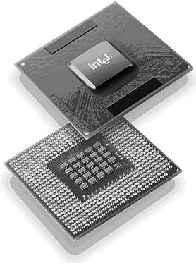 The main technical details for the Pentium 4-M include these: -
Speeds that range from 1.3GHz to 3.2GHz and beyond -
55 million transistors , 0.13-micron process, 131mm 2 die (Northwood, see Figure 4.16) Figure 4.16. Pentium 4 Northwood die (0.13-micron process, 55 million transistors, 131mm 2 ). ( Photograph used by permission of Intel Corporation.) 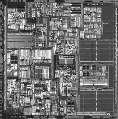 -
Software compatible with previous Intel 32-bit processors -
Processor (front-side) bus that runs at 400MHz -
Arithmetic logic units (ALUs) that run at twice the processor core frequency -
Hyperpipelined (20-stage) technology -
Very deep out-of-order instruction execution -
Enhanced branch prediction -
20KB L1 cache (12KB L1 execution trace cache plus 8KB L1 data cache) -
512KB of on-die, full-core speed 128-bit L2 cache with eight-way associativity -
L2 cache that can handle up to 4GB RAM and that supports ECC -
SSE2 ”144 new SSE2 instructions for graphics and sound processing -
Enhanced floating-point unit -
Multiple low-power states Intel has abandoned Roman numerals for a standard Arabic numeral 4 designation. Internally, the Pentium 4-M introduces a new architecture that Intel calls NetBurst microarchitecture, which is a marketing term, not a technical term . Intel uses NetBurst to describe hyperpipelined technology, a rapid-execution engine, a high-speed (400MHz) system bus, and an execution trace cache. The hyperpipelined technology doubles the instruction pipeline depth as compared to the Pentium III, meaning that more and smaller steps are required to execute instructions. This might seem less efficient, but it enables much higher clock speeds to be more easily attained. The rapid-execution engine enables the two integer arithmetic logic units (ALUs) to run at twice the processor core frequency, which means that instructions can execute in half a clock cycle. The 400MHz system bus is a quad-pumped bus running off a 100MHz system clock transferring data four times per clock cycle. The execution trace cache is a high-performance Level 1 cache that stores approximately 12KB decoded micro-operations. This removes the instruction decoder from the main execution pipeline, increasing performance. Of these, the high-speed processor bus is most notable. Technically, the processor bus is a 100MHz quad-pumped bus that transfers four times per cycle (4x), for a 400MHz effective rate. Because the bus is 64 bits (8 bytes) wide, this results in a throughput rate of 3200MBps. In the new 20-stage pipelined internal architecture, individual instructions are broken down into many more substages, making this almost like a RISC processor. Unfortunately, this can add to the number of cycles taken to execute instructions if they are not optimized for this processor. Early benchmarks running existing software showed that existing Pentium III or AMD Athlon processors could easily keep pace with or even exceed the Pentium 4 in specific tasks ; however, this is changing now that applications are being recompiled to work smoothly with the Pentium 4's deep pipelined architecture. When used in conjunction with the requisite Intel SpeedStep technology driver, the Mobile Pentium 4-M supports Enhanced SpeedStep technology, which enables real-time dynamic switching of the voltage and frequency between two performance modes. This allows switching of the bus ratios, core operating voltage, and core processor speeds without resetting the system. The Mobile Pentium 4 Processor-M is available at the speeds listed in Table 4.8. Table 4.8. Mobile Pentium 4-M Processor Speed and Power Consumption | Maximum Performance | Battery-Optimized Mode | | Processor Frequency | Voltage | Power Consumption | Optimized Speed | Voltage | Power Consumption | | 2.60GHz | 1.3V | 35W | 1.20GHz | 1.2V | 20.8W | | 2.50GHz | 1.3V | 35W | 1.20GHz | 1.2V | 20.8W | | 2.40GHz | 1.3V | 35W | 1.20GHz | 1.2V | 20.8W | | 2.20GHz | 1.3V | 35W | 1.20GHz | 1.2V | 20.8W | | 2.0GHz | 1.3V | 32W | 1.20GHz | 1.2V | 20.8W | | 1.90GHz | 1.3V | 32W | 1.20GHz | 1.2V | 20.8W | | 1.80GHz | 1.3V | 30W | 1.20GHz | 1.2V | 20.8W | | 1.70GHz | 1.3V | 24.5W | 1.20GHz | 1.2V | 20.8W | | 1.60GHz | 1.3V | 30W | 1.20GHz | 1.2V | 20.8W | | 1.50GHz | 1.3V | 26.9W | 1.20GHz | 1.2V | 20.8W | | 1.40GHz | 1.3V | 25.8W | 1.20GHz | 1.2V | 20.8W | In June 2003, Intel introduced the Mobile Pentium 4, which is different from the Mobile Pentium 4-M that preceded it. The main differences between the Mobile Pentium 4 and the Mobile Pentium 4-M are shown Table 4.9. Table 4.9. Mobile Pentium 4-M and Mobile Pentium 4 Processor Differences | Feature | Mobile Pentium 4-M | Mobile Pentium 4 | | Bus speed | 400MHz | 533MHz | | CPU speed | Up to 2.6GHz | Up to 3.2GHz | | SpeedStep | Yes | Yes | | Hyperthreading | No | Optional | | Voltage | 1.3/1.2V | 1.5/1.2V | | Power | 35W | 70W | The Mobile Pentium 4 is based on the desktop Pentium 4 processor but is designed to run on a marginally lower voltage and with the addition of enhanced SpeedStep. This processor is designed for high- powered laptops that are used more as transportable desktop systems, in which battery life is not a big concern. Although this is close to being a desktop chip, it still offers power-management and reduced voltage operation features that make it much more suitable for use in a laptop than the full desktop version of the Pentium 4. Table 4.10 shows the specifications for the Mobile Pentium 4 processors. Table 4.10. Mobile Pentium 4 Processor Specifications | CPU Max Speed | CPU Min Speed | CPU Bus Speed | S-Spec | Power (Watts) | | 3.06GHz | 1.6GHz | 533MHz | SL726 | 70 | | 2.80GHz | 1.6GHz | 533MHz | SL725 | 68.4 | | 2.66GHz | 1.6GHz | 533MHz | SL724 | 66.1 | | 2.40GHz | 1.6GHz | 533MHz | SL723 | 59.8 | Pentium M The Pentium M is the first Intel processor designed exclusively for mobile use. The Pentium M processor (code-named Banias) was officially introduced in March 2003 along with the 855 chipset family and the PRO/Wireless 2100 mini-PCI network adapter, which fall under what Intel calls the Centrino brand name when combined in a single system. Figure 4.17 shows all of the components that make up the Centrino brand. Figure 4.17. Pentium M and Centrino Components. ( Photograph used by permission of Intel Corporation.) 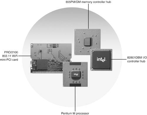 The core of Centrino is the Pentium M processor, which, in many ways, seems to be a combination of the best features of both the Pentium III and Pentium 4 processor cores, with a Pentium 4 bus and other major enhancements and features added. The major enhancements come in the form of several new internal architectural features, including the following: -
Micro-operation fusion. Micro-operations derived from the same instruction or macro-operation are fused together, resulting in greater throughput using less power. -
ESP (Extended Stack Pointer) Folding. High-level code often requires intensive stack manipulation. ESP Folding eliminates ESP-manipulation micro-operations in stack- related operations, enabling faster execution. -
32KB L1 cache. -
Massive 1MB on-die L2 cache (twice as large as the Pentium III/4 cache). -
Wider queues and translation lookaside buffers (TLBs). -
128 entries in TLBs. -
Improved branch prediction. The Pentium M offers performance equal to or even greater than that of the Pentium 4, while consuming much less power and generating much less heat. Other features include these: -
77 million transistors, 0.13-micron process, and 84mm 2 die (Northwood, see Figure 4.16) -
Software compatible with previous Intel 32-bit processors -
Processor (front-side) bus that runs at 400MHz -
SSE2 ”144 new SSE2 instructions for graphics and sound processing -
Enhanced floating-point unit -
Multiple low-power states, including the capability to power off portions of the processor and cache that aren't being used The Pentium M processor with the Banias core contains 77 million transistors and is manufactured using 0.13-micron process technology. It is available in speeds ranging from 1.3GHz to 1.7GHz. A version with a new Dothan core using 0.09-micron technology is available at 1.8GHz. The Pentium M includes Enhanced SpeedStep technology with multiple voltage and frequency operating points to conserve power and Streaming SIMD Extensions 2 (SSE2), which is the latest version of MMX technology also included with the Pentium 4. The Pentium M die is shown in Figure 4.18. Figure 4.18. Pentium M Die, 0.13 micron Banias Core. ( Photograph used by permission of Intel Corporation.) 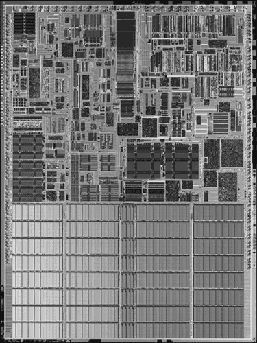 Notice that the Pentium M die is dominated by the huge 1MB L2 cache, which takes up nearly half the space on the chip. The large cache is responsible for the high transistor count because, in general, it takes about six transistors for each bit of cache memory. Table 4.11 lists the various models of the Pentium M processors that Intel has released. Table 4.11. Pentium M Processor Models and Revisions | CPU Max Speed | CPU Min Speed | Bus Speed | S-Spec | Stepping | CPUID | L2 | Power (Watts) | | 1.30GHz | 600MHz | 400MHz | SL6N4 | PB1 | 0695 | 1MB | 22.0 | | 1.40GHz | 600MHz | 400MHz | SL6F8 | PB1 | 0695 | 1MB | 22.0 | | 1.50GHz | 600MHz | 400MHz | SL6F9 | PB1 | 0695 | 1MB | 24.5 | | 1.60GHz | 600MHz | 400MHz | SL6FA | PB1 | 0695 | 1MB | 24.5 | | 1.70GHz | 600MHz | 400MHz | SL6N5 | PB1 | 0695 | 1MB | 24.5 | A Centrino by Any Other Name The name Pentium M refers only to the actual processor, while the name Centrino refers to the combination of the Pentium M processor, 855 chipset, and the Intel PRO/2100 mini-PCI wireless network card. Laptops can be assembled using the Pentium M processor and 855 chipset, and with a non-Intel wireless card; however, according to Intel's marketing rules, the Centrino brand name or sticker can't be applied in such a case. Because there is no direct connection between the wireless networking card and the processor or chipset, the Centrino brand name is merely Intel's method of forcing its way into the wireless networking business and is really unrelated to the Pentium M processor itself. Note that many of the third-party wireless network cards (such as those from Atheros or Agere) offer equal or better performance and power consumption as Intel's own card. In other words, if you want the ultimate in laptop performance and battery life, look for the Pentium M processor with or without the entire Centrino branded package. |
Because of the high-speed bus, large internal cache, and shorter internal pipeline (similar to the Pentium III), the Pentium M performs much faster than its raw clock speed indicates. Intel performance tests on the Mobile Pentium 4, Mobile Pentium 4-M, and Pentium M show that the Pentium M is significantly faster than you might think, as seen in Table 4.12. Table 4.12. Comparison of MobilMark 2002 Scores and Relative Battery Life Among Mobile Pentium 4, Mobile Pentium 4-M, and Pentium M Processors | CPU Type | CPU Speed | Bus Speed | MobilMark 2002 Score | Relative Battery Life | | Mobile Pentium 4 | 3.06GHz | 533MHz | 216 | 2.43 | | Mobile Pentium 4 | 2.40GHz | 533MHz | 197 | 2.62 | | Pentium M | 1.70GHz | 400MHz | 195 | 4.66 | | Mobile Pentium 4-M | 2.60GHz | 400MHz | 179 | 2.80 | | Mobile Pentium 4-M | 2.00GHz | 400MHz | 163 | 2.80 | | Mobile Pentium 4-M | 1.40GHz | 400MHz | 142 | 2.87 | From this table, you can see that the 1.7GHz Pentium M is significantly faster than the 2.6GHz Mobile Pentium 4-M and is just about tied with the 2.4GHz Mobile Pentium 4, while offering nearly double the battery life! One thing not shown on this table is how cool the Pentium M actually runs. Most of the Pentium 4 laptops I've used get uncomfortably hot if you actually have them sitting on your lap. The Pentium M, on the other hand, uses much less power and, as a result, generates much less heat so that the system exterior barely gets warm to the touch. A fringe benefit of this is that Pentium M systems are inherently quiet because they don't need a roaring fan to keep them cool. If you want a fast, cool, and quiet laptop, I highly recommend systems using the Pentium M processor. Mobile Celeron Processors The mobile Celeron processor is available in several versions, including those based on Pentium II, Pentium III, and Pentium 4 processors. The 1.4GHz and faster versions of the mobile Celeron processor are based on the Mobile Pentium 4 design. They are essentially identical to Mobile Pentium 4 processors, except that they include only 256KB of L2 cache. Like the Mobile Pentium 4, these chips utilize a 478-pin, micro-FCPGA package and plug into a micro-479 PGA mobile (mPGA479M) socket. The Pentium 4 “based mobile Celeron is designed for low-cost, high-value portable systems. Features of the processor are the same as the Pentium 4, with the exception of cache size and, in some cases, bus speed. Mobile Celeron processors based on the Pentium 4 design are available at the following core speeds: -
2.2GHz -
2.0GHz -
1.8GHz -
1.7GHz -
1.6GHz -
1.5GHz -
1.4GHz All of these processors use the 400MHz Pentium 4 bus. Mobile Celeron processors from 650MHz through 1.33GHz are built on a 0.13-micron process, available in both micro-FCBGA and micro-FCPGA packages, and use the same core as the Mobile Pentium III. As with the Pentium III, these processors include Streaming SIMD instructions, an Advanced Transfer Cache architecture, and a processor system bus speed of 100 or 133MHz. These features are offered in micro-FCPGA and micro-FCBGA packages. The Low Voltage and Ultra Low Voltage mobile processors will be available only in the micro-FCBGA package. The 256KB integrated L2 cache based on the Advanced Transfer Cache architecture runs at full core speed. Mobile Celeron processors based on the 0.13-micron Pentium III design with 256KB of L2 cache are available at the following speeds: -
1.33GHz -
1.26GHz -
1.20GHz -
1.13GHz -
1.06GHz -
1.00GHz -
733MHz -
700MHz -
667MHz -
650MHz Mobile Celeron processors from 400MHz through 900MHz are built on a 0.18-micron process, available in micro-BGA2 and micro-PGA2 packages, and use the same core as the Pentium III, but with only 128KB of L2 cache. Mobile Celeron processor based on the 0.18-micron Pentium III design are available in the following core speeds: -
900MHz -
850MHz -
800MHz -
750MHz -
700MHz -
650MHz -
600MHz -
550MHz -
500MHz -
450MHz -
400MHz All of these processors use a 100MHz Pentium III bus. Mobile Celeron processors from 733MHz to 933MHz use a 0.18-micron process and micro-FCBGA or micro-FCPGA packages. These processors support a bus speed of 133MHz and a 128KB L2 cache, and are offered in micro-FCBGA and micro-FCPGA form factors. Mobile Celeron processor based on the 0.18-micron Pentium III design are available in the following core speeds: -
933MHz -
866MHz -
800AMHz -
733MHz The "A" designation indicates a 133MHz bus, to differentiate the same-speed model with a slower 100MHz bus. Mobile Celeron Processors and Steppings Intel's entry into low-cost processors, the Celeron, is also available in a mobile form, featuring reduced voltages, PGA or BGA (ball grid array) packaging, and the MMC-1 and MMC-2 minicartridge modules also used by the Mobile Pentium III. Table 4.13 lists the steppings for Mobile Celeron processors in BGA and PGA packaging. Table 4.13. Mobile Celeron Processor Steppings | Family | Model | Core Stepping | L2 Cache (KB) | S-Spec | Speed Core/Bus | Notes | | 6 | 6 | mcbA0 | 128 | SL23X | 266/66 | B, 1 | | 6 | 6 | mcbA0 | 128 | SL23Y | 266/66 | B, 1 | | 6 | 6 | mcbA0 | 128 | SL3AH | 300/66 | B, 1 | | 6 | 6 | mcbA0 | 128 | SL3C8 | 333/66 | B, 1 | | 6 | 6 | mcbA0 | 128 | SL3C7 | 366/66 | B, 1 | | 6 | 6 | mcbA0 | 128 | SL3DQ | 266/66 | B, 2 | | 6 | 6 | mcbA0 | 128 | SL3GQ | 400/66 | B, 1 | | 6 | 6 | mcbA0 | 128 | SL3KA | 433/66 | P, 1 | | 6 | 6 | mcbA0 | 128 | SL3KC | 466/66 | P, 1 | | 6 | 6 | mcpA0 | 128 | SL3HM | 266/66 | P, 1 | | 6 | 6 | mcpA0 | 128 | SL3HN | 300/66 | P, 1 | | 6 | 6 | mcpA0 | 128 | SL3HP | 333/66 | P, 1 | | 6 | 6 | mcpA0 | 128 | SL3HQ | 366/66 | P, 1 | | 6 | 6 | mcpA0 | 128 | SL3GR | 400/66 | P, 1 | | 6 | 6 | mcpA0 | 128 | SL3KB | 433/66 | P, 1 | | 6 | 6 | mcpA0 | 128 | SL3KD | 466/66 | P, 1 | | B = BGA package | | P = PGA package | | 1 = Runs at a core voltage of 1.6V | | 2 = Runs at a core voltage of 1.5V | Table 4.14 lists the steppings for Mobile Celeron processors in MMC-1 and MMC-2 minicartridge packaging. All Mobile Celerons in MMC-1 and MMC-2 packaging also feature a 128KB L1 cache. Table 4.14. Mobile Celeron Minicartridge Steppings | Speed Core/Bus | Product Stepping | CPUID | PTC | Package | | 266/66 | cmmA0 | 066A | PMH26601001AA | MMC-1 | | 266/66 | cmmA0 | 066A | PMH26601001AA | MMC-1 | | 300/66 | cmmA0 | 066A | PMH30001001AA | MMC-1 | | 333/66 | cmmA0 | 066A | PMH33301001AA | MMC-1 | | 366/66 | cmmA0 | 066A | PMH36601001AA | MMC-1 | | 400/66 | cmmA0 | 066A | PMH40001001AA | MMC-1 | | 433/66 | cmmA0 | 066A | PMH43301001AA | MMC-1 | | 466/66 | cmmA0 | 066A | PMH46601001AA | MMC-1 | | 266/66 | cmmA0 | 066A | PMI26601001AA | MMC-2 | | 300/66 | cmmA0 | 066A | PMI30001001AA | MMC-2 | | 333/66 | cmmA0 | 066A | PMI33301001AA | MMC-2 | | 366/66 | cmmA0 | 066A | PMI36601001AA | MMC-2 | | 400/66 | cmmA0 | 066A | PMI40001001AA | MMC-2 | | 433/66 | cmmA0 | 066A | PMI43301001AA | MMC-2 | | 466/66 | cmmA0 | 066A | PMI46601001AA | MMC-2 | The latest Mobile Celeron processors are built on the same 0.18-micron process and the same micro-BGA2 and micro-PGA2 packaging used by the Pentium III processor, and feature a bus speed of 100MHz, which is faster than previous Mobile Celeron CPUs. Table 4.15 lists the steppings for 0.18-micron Mobile Celeron processors in micro-BGA2 or micro-PGA2 packaging. Table 4.15. Mobile Celeron Processor (0.18 Micron) Steppings | Speed (MHz) Core/Bus | S-Spec | Product Stepping | CPUID | L2 Cache Size | Package | | 400/100 | SL3UL | BA2 | 0681 | 128KB | BGA2 | | 400/100 | SL43W | BB0 | 0683 | 128KB | BGA2 | | 400/100 | SL4J8 | BC0 | 0686 | 128KB | BGA2 | | 450/100 | SL3PD | BA2 | 0681 | 128KB | BGA2 | | 450/100 | SL43T | BB0 | 0683 | 128KB | BGA2 | | 450/100 | SL4JC | BC0 | 0686 | 128KB | BGA2 | | 450/100 | SL3PF | PA2 | 0681 | 128KB | mPGA2 | | 450/100 | SL43U | PB0 | 0683 | 128KB | mPGA2 | | 450/100 | SL4JS | PC0 | 0686 | 128KB | mPGA2 | | 500/100 | SL45A | BB0 | 0683 | 128KB | BGA2 | | 500/100 | SL3PC | BA2 | 0681 | 128KB | BGA2 | | 500/100 | SL43Q | BB0 | 0683 | 128KB | BGA2 | | 500/100 | SL4JD | BC0 | 0686 | 128KB | BGA2 | | 500/100 | SL4J9 | BC0 | 0686 | 128KB | BGA2 | | 500/100 | SL4ZR | BC0 | 0686 | 128KB | BGA2 | | 500/100 | SL5DR | BD0 | 068A | 128KB | BGA2 | | 500/100 | SL3PE | PA2 | 0681 | 128KB | mPGA2 | | 500/100 | SL43R | PB0 | 0683 | 128KB | mPGA2 | | 500/100 | SL4JT | PC0 | 0686 | 128KB | mPGA2 | | 550/100 | SL3ZE | BB0 | 0683 | 128KB | BGA2 | | 550/100 | SL4JE | BC0 | 0686 | 128KB | BGA2 | | 550/100 | SL3ZF | PB0 | 0683 | 128KB | mPGA2 | | 550/100 | SL4JU | PC0 | 0686 | 128KB | mPGA2 | | 600/100 | SL4AR | BB0 | 0683 | 128KB | BGA2 | | 600/100 | SL4JF | BC0 | 0686 | 128KB | BGA2 | | 600/100 | SL5DS | BD0 | 068A | 128KB | BGA2 | | 600/100 | SL582 | BD0 | 068A | 128KB | BGA2 | | 600/100 | SL4AP | PB0 | 0683 | 128KB | mPGA2 | | 600/100 | SL4JV | PC0 | 0686 | 128KB | mPGA2 | | 650/100 | SL4AD | BB0 | 0683 | 128KB | BGA2 | | 650/100 | SL4JG | BC0 | 0686 | 128KB | BGA2 | | 650/100 | SL4AE | PB0 | 0683 | 128KB | mPGA2 | | 650/100 | SL4JW | PC0 | 0686 | 128KB | mPGA2 | | 700/100 | SL4GU | BC0 | 0686 | 128KB | BGA2 | | 700/100 | SL53V | BD0 | 068A | 128KB | BGA2 | | 700/100 | SL4GX | PC0 | 0686 | 128KB | mPGA2 | | 700/100 | SL53D | PD0 | 068A | 128KB | mPGA2 | | 750/100 | SL56P | BC0 | 0686 | 128KB | BGA2 | | 750/100 | SL53U | BD0 | 068A | 128KB | BGA2 | | 750/100 | SL56Q | PC0 | 0686 | 128KB | mPGA2 | | 750/100 | SL53C | PD0 | 068A | 128KB | mPGA2 | | 800/100 | SL57X | BD0 | 068A | 128KB | BGA2 | | 800/100 | SL584 | PD0 | 068A | 128KB | mPGA2 |  |