Processor Features
| As new processors are introduced, new features are continually added to their architectures to help improve everything from performance in specific types of applications to the reliability of the CPU as a whole. The next few sections take a look at some of these technologies, including System Management Mode (SMM), Superscalar Execution, MMX, SSE, 3DNow!, and HT Technology. SMM (Power Management)Spurred on primarily by the goal of putting faster and more powerful processors in laptop computers, and yet maintaining reduced power consumption and decent battery life, Intel has created power-management circuitry. This circuitry enables processors to conserve energy use and lengthen battery life. This was introduced initially in the Intel 486SL processor, which is an enhanced version of the 486DX processor. Subsequently, the power-management features were universalized and incorporated into all Pentium and later processors. This feature set is called SMM, which stands for System Management Mode . SMM circuitry is integrated into the physical chip but operates independently to control the processor's power use based on its activity level. It enables the user to specify time intervals after which the CPU will be partially or fully powered down. It also supports the Suspend/Resume feature that allows for instant power on and power off, used mostly with laptop PCs. These settings are typically controlled via system BIOS settings. Superscalar ExecutionThe fifth-generation Pentium and newer processors feature multiple internal instruction-execution pipelines, which enable them to execute multiple instructions at the same time. The 486 and all preceding chips can perform only a single instruction at a time. Intel calls the capability to execute more than one instruction at a time superscalar technology. This technology provides additional performance compared with the 486. Superscalar architecture usually is associated with high-output Reduced Instruction Set Computer (RISC) chips. A RISC chip has a less complicated instruction set with fewer and simpler instructions. Although each instruction accomplishes less, overall the clock speed can be higher, which can usually increase performance. The Pentium is one of the first Complex Instruction Set Computer (CISC) chips to be considered superscalar. A CISC chip uses a richer, fuller -featured instruction set, which has more complicated instructions. As an example, say that you wanted to instruct a robot to screw in a light bulb. Using CISC instructions, you would say this:
Using RISC instructions, you would say something more along the lines of this:
Overall, many more RISC instructions are required to do the job because each instruction is simpler (reduced) and does less. The advantage is that the robot (or processor) must deal with fewer overall commands and can execute the individual commands more quicklyand, thus, in many cases, execute the complete task (or program) more quickly as well. The debate goes on whether RISC or CISC is better, but, in reality, there is no such thing as a pure RISC or CISC chipit is all just a matter of definition, and the lines are somewhat arbitrary. Intel and compatible processors have generally been regarded as CISC chips, although the fifth- and sixth -generation versions have many RISC attributes and internally break down CISC instructions into RISC versions. MMX TechnologyIntel introduced MMX technology in January 1997 for both desktop and mobile Pentium processors. MMX was originally named for multimedia extensions or matrix math extensions, depending on whom you ask. Intel officially states that it is actually not an abbreviation and stands for nothing other than the letters MMX (not being an abbreviation was apparently required so that the letters could be trademarked); however, the internal origins are probably one of the preceding. MMX technology was introduced in the later fifth-generation Pentium processors as a kind of add-on that improves video compression/ decompression , image manipulation, encryption, and I/O processingall of which are used in a variety of today's software. MMX consists of two main processor architectural improvements. The first is very basic; all MMX chips have a larger internal L1 cache than their non-MMX counterparts. This improves the performance of any and all software running on the chip, regardless of whether it actually uses the MMX-specific instructions. The other part of MMX is that it extends the processor instruction set with 57 new commands or instructions, as well as a new instruction capability called single instruction, multiple data (SIMD). Modern multimedia and communication applications often use repetitive loops that occupy 10% or less of the overall application code but can account for up to 90% of the execution time. SIMD enables one instruction to perform the same function on multiple pieces of data, similar to a teacher telling an entire class to sit down rather than addressing each student one at a time. SIMD enables the chip to reduce processor- intensive loops common with video, audio, graphics, and animation. Intel also added 57 new instructions specifically designed to manipulate and process video, audio, and graphical data more efficiently . These instructions are oriented to the highly parallel and often repetitive sequences frequently found in multimedia operations. Highly parallel refers to the fact that the same processing is done on many data points, such as when modifying a graphic image. The main drawbacks to MMX were that it worked only on integer values and used the floating-point unit for processing, so time was lost when a shift to floating-point operations was necessary. These drawbacks were corrected in the additions to MMX from Intel and AMD. Intel licensed the MMX capabilities to competitors such as AMD and Cyrix, which were then able to upgrade their own Intel-compatible processors with MMX technology. SSE and SSE2In February 1999, Intel introduced the Pentium III processor and included in that processor an update to MMX called Streaming SIMD Extensions (SSE). These were also called Katmai New Instructions (KNI) until their debut because they were originally included on the Katmai processor, which was the code name for the Pentium III. The Celeron 533A and faster Celeron processors based on the Pentium III core also support SSE instructions. The earlier Pentium II and Celeron 533 and lower (based on the Pentium II core ) do not support SSE. SSE includes 70 new instructions for graphics and sound processing over what MMX provided. SSE is similar to MMX; in fact, besides being called KNI, SSE was also called MMX-2 by some before it was released. In addition to adding more MMX style instructions, the SSE instructions allow for floating-point calculations and now use a separate unit within the processor instead of sharing the standard floating-point unit as MMX did. SSE2 was introduced in November 2000, along with the Pentium 4 processor, and adds 144 additional SIMD instructions. SSE2 also includes all the previous MMX and SSE instructions. The Streaming SIMD Extensions consist of new instructions, including SIMD floating-point, additional SIMD integer, and cacheability control instructions. Some of the technologies that benefit from the Streaming SIMD Extensions include advanced imaging, 3D video, streaming audio and video (DVD playback), and speech-recognition applications. The benefits of SSE include the following:
The SSE and SSE2 instructions are particularly useful with MPEG2 decoding, which is the standard scheme used on DVD video discs. SSE-equipped processors should therefore be more capable of performing MPEG2 decoding in software at full speed without requiring an additional hardware MPEG2 decoder card. SSE-equipped processors are much better and faster than previous processors when it comes to speech recognition as well. One of the main benefits of SSE over plain MMX is that it supports single-precision floating-point SIMD operations, which have posed a bottleneck in the 3D graphics processing. Just as with plain MMX, SIMD enables multiple operations to be performed per processor instruction. Specifically, SSE supports up to four floating-point operations per cycle; that is, a single instruction can operate on four pieces of data simultaneously . SSE floating-point instructions can be mixed with MMX instructions with no performance penalties. SSE also supports data prefetching , which is a mechanism for reading data into the cache before it is actually called for. Note that for any of the SSE instructions to be beneficial, they must be encoded in the software you are using, so SSE-aware applications must be used to see the benefits. Most software companies writing graphics- and sound- related software today have updated those applications to be SSE aware and use the features of SSE. For example, high-powered graphics applications such as Adobe Photoshop support SSE instructions for higher performance on processors equipped with SSE. Microsoft includes support for SSE in its DirectX 6.1 and later video and sound drivers, which are included with Windows 98 Second Edition, Windows Me, Windows NT 4.0 (with service pack 5 or later), Windows 2000, and Windows XP. SSE is an extension to MMX, and SSE2 is an extension to SSE; therefore, processors that support SSE2 also support the SSE instructions, and processors that support SSE also support the original MMX instructions. This means that standard MMX-enabled applications run as they did on MMX-only processors. 3DNow!, Enhanced 3DNow!, and 3DNow! Professional3DNow! technology was originally introduced as AMD's alternative to the SSE instructions in the Intel processors. Actually, 3DNow! was first introduced in the K6 series before Intel released SSE in the Pentium III and then AMD added Enhanced 3DNow! to the Athlon and Duron processors. The latest version, 3DNow! Professional, was introduced in the first Athlon XP processors. AMD licensed MMX from Intel, and all its K6 series, Athlon, Duron, and later processors include full MMX instruction support. Not wanting to additionally license the SSE instructions being developed by Intel, AMD first came up with a different set of extensions beyond MMX called 3DNow!. Introduced in May 1998 in the K6-2 processor and enhanced when the Athlon was introduced in June 1999, 3DNow! and Enhanced 3DNow! are sets of instructions that extend the multimedia capabilities of the AMD chips beyond MMX. This enables greater performance for 3D graphics, multimedia, and other floating pointintensive PC applications. 3DNow! technology is a set of 21 instructions that use SIMD techniques to operate on arrays of data rather than single elements. Enhanced 3DNow! adds 24 more instructions (19 SSE and 5 DSP/communcations instructions) to the original 21, for a total of 45 new instructions. Positioned as an extension to MMX technology, 3DNow! is similar to the SSE found in the Pentium III and Celeron processors from Intel. According to AMD, 3DNow! provides approximately the same level of improvement to MMX as did SSE, but in fewer instructions with less complexity. Although similar in capability, they are not compatible at the instruction level, so software specifically written to support SSE does not support 3DNow!, and vice versa. The latest version of 3DNow!, 3DNow! Professional, adds 51 SSE commands to 3DNow! Enhanced, meaning that 3DNow! Professional now supports all SSE commands; as a result, AMD chips now essentially have SSE capability. Unfortunately, AMD does not yet include SSE2, which is currently found only on the Pentium 4 and Pentium 4based Celeron processors. Just as with SSE, 3DNow! supports single-precision floating-point SIMD operations and enables up to four floating-point operations per cycle. 3DNow! floating-point instructions can be mixed with MMX instructions with no performance penalties. 3DNow! also supports data prefetching. Also like SSE, 3DNow! is well supported by software, including Windows 9 x , Windows NT 4.0, and all newer Microsoft operating systems. 3DNow!specific support is no longer a big issue if you are using an Athlon XP or Athlon 64 processor because they now fully support SSE through their support of 3DNow! Professional. Dynamic ExecutionFirst used in the P6 or sixth-generation processors (including the Pentium Pro, Pentium II/III, and Celeron processors based on the Pentium II and III designs), dynamic execution enables the processor to execute more instructions in parallel so that tasks are completed more quickly. This technology innovation is comprised of three main elements:
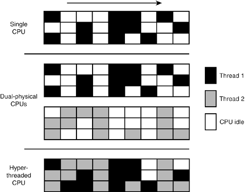
Branch PredictionBranch prediction is a feature formerly found only in high-end mainframe processors. It enables the processor to keep the instruction pipeline full while running at a high rate of speed. A special fetch/decode unit in the processor uses a highly optimized branch-prediction algorithm to predict the direction and outcome of the instructions being executed through multiple levels of branches, calls, and returns. It is similar to a chess player working out multiple strategies before game play by predicting the opponent 's strategy several moves into the future. By predicting the instruction outcome in advance, the instructions can be executed with no waiting. Data Flow AnalysisData flow analysis studies the flow of data through the processor to detect any opportunities for out-of-order instruction execution. A special dispatch/execute unit in the processor monitors many instructions and can execute these instructions in an order that optimizes the use of the multiple superscalar execution units. The resulting out-of-order execution of instructions can keep the execution units busy even when cache misses and other data-dependent instructions might otherwise hold things up. Speculative ExecutionSpeculative execution is the processor's capability to execute instructions in advance of the actual program counter. The processor's dispatch/execute unit uses data flow analysis to execute all available instructions in the instruction pool and store the results in temporary registers. A retirement unit then searches the instruction pool for completed instructions that are no longer data-dependent on other instructions to run or that have unresolved branch predictions . If any such completed instructions are found, the results are committed to memory by the retirement unit or the appropriate standard Intel architecture in the order they were originally issued. They are then retired from the pool. Dynamic execution essentially removes the constraint and dependency on linear instruction sequencing. By promoting out-of-order instruction execution, it can keep the instruction units working rather than waiting for data from memory. Even though instructions can be predicted and executed out of order, the results are committed in the original order, to avoid disrupting or changing program flow. This enables the processors in the P6 generation to run existing Intel architecture software exactly as the Pentium (P5 generation) and previous processors didjust a whole lot more quickly! Dual Independent Bus ArchitectureThe Dual Independent Bus (DIB) architecture was another innovation that was first implemented in the sixth-generation processors from Intel and AMD. DIB was created to improve processor bus bandwidth and performance. Having two (dual) independent data I/O buses enables the processor to access data from either bus simultaneously and in parallel rather than in a singular sequential manner (as in a single-bus system). The main (often called front-side) processor bus is the interface between the processor and the motherboard or chipset. The second (back-side) bus in a processor with DIB is used for the L2 cache, enabling it to run at much greater speeds than if it shared the main processor bus. Two buses make up the DIB architecture: the L2 cache bus and the main CPU bus, often called the FSB (front-side bus). The P6 class processors from the Pentium Pro to the Celeron, Pentium II/III/4, and Athlon/Duron processors can use both buses simultaneously, eliminating a bottleneck there. The dual-bus architecture enables the L2 cache of the newer processors to run at full speed inside the processor core on an independent bus, leaving the main CPU bus (FSB) to handle normal data flowing into and out of the chip. The two buses run at different speeds. The front-side bus or main CPU bus is coupled to the speed of the motherboard, whereas the back-side or L2 cache bus is coupled to the speed of the processor core. As the frequency of processors increases, so does the speed of the L2 cache. The key to implementing DIB was to move the L2 cache memory off the motherboard and into the processor package. L1 cache always has been a direct part of the processor die, but L2 was larger and originally had to be external. By moving the L2 cache into the processor, the L2 cache could run at speeds more like the L1 cache, much faster than the motherboard or processor bus. DIB also enables the system bus to perform multiple simultaneous transactions (instead of singular sequential transactions), accelerating the flow of information within the system and boosting performance. Overall, DIB architecture offers up to three times the bandwidth performance over a single-bus architecture processor. Hyperthreading TechnologyComputers with two or more physical processors have long had a performance advantage over single-processor computers when the operating system supports multiple processors, as is the case with Windows NT 4.0, 2000, XP Professional, and Linux. However, dual-processor motherboards and systems have always been more expensive than otherwise-comparable single-processor systems, and upgrading a dual-processorcapable system to dual-processor status can be difficult because of the need to match processor speeds and specifications. However, Intel's new Hyperthreading (HT) Technology allows a single processor to handle two independent sets of instructions at the same time. In essence, HT Technology converts a single physical processor into two virtual processors. Intel originally introduced HT Technology in its line of Xeon processors for servers in March 2002. HT Technology enables multiprocessor servers to act as if they had twice as many processors installed. HT Technology was introduced on Xeon workstation-class processors with a 533MHz system bus and found its way into PC processors with the 3.06GHz Pentium 4 processor in November 2002. Since then, HT Technology has appeared on desktop Pentium 4 processors from 2.4GHz through 3.6GHz, and mobile Pentium 4 processors from 2.66GHz through 3.46GHz, with the faster ones using the new Prescott core. How Hyperthreading WorksInternally, an HT-enabled processor has two sets of general-purpose registers, control registers, and other architecture components , but both logical processors share the same cache, execution units, and buses. During operations, each logical processor handles a single thread (see Figure 4.14). Figure 4.14. A processor with HT Technology enabled can fill otherwise-idle time with a second process, improving multitasking and performance of multithreading single applications. Although the sharing of some processor components means that the overall speed of an HT-enabled system isn't as high as a true dual-processor system would be, speed increases of 25% or more are possible when multiple applications or a single multithreaded application is being run. Hyperthreading RequirementsThe first HT-enabled PC processor is the Intel 3.06GHz Pentium 4. All faster Pentium 4 models also support HT Technology, as do all processors 2.4GHz and faster that use the 800MHz bus. However, an HT-enabled Pentium 4 processor by itself can't bring the benefits of HT Technology to your system. You also need the following:
Although Windows NT 4.0 and Windows 2000 are designed to use multiple physical processors, HT Technology requires specific operating system optimizations to work correctly. Linux distributions based on kernel 2.4.18 and higher also support HT Technology. Early test results indicate that HT Technology already provides a good performance boost in existing applications. After applications are rewritten to be HT-aware, performance increases still further. |
EAN: 2147483647
Pages: 182