Server Chipsets Overview
| The chipset typically contains the processor bus interface (called the front-side bus [FSB]), memory controllers, bus controllers, I/O controllers, and more. All the circuits on the motherboard are contained within the chipset. If the CPU is like the engine in your car, the chipset represents the car's chassis. It is the framework in which the engine rests and is its connection to the outside world. The chipset is the frame, suspension, steering, wheels and tires, transmission, driveshaft, differential, and brakes. The chassis in your car is what gets the power to the ground, allowing the vehicle to start, stop, and corner. In a typical server, the chipset represents the connection between the processor and everything else. In most cases, the processor can't talk to memory modules, adapter boards, devices, and so on without going through the chipset. Note The AMD Opteron processors for servers and workstations incorporate memory controllers. Thus, chipsets that support Opteron processors do not contain memory controllers. Because the chipset controls the interface or connections between the processor and everything else, the chipset ends up dictating which type of processor you have; how fast it will run; how fast each bus will operate; the speed, type, and amount of memory you can use; and more. In fact, the chipset might be the single most important component in a system, possibly even more important than the processor. Systems with faster processors can be outperformed by systems with slower processors but better chipsets, much like how a car with less power might win a race through better cornering, acceleration, and braking. When deciding on an x86 server, whether it is prebuilt or assembled from parts, it is a good idea to start by choosing the chipset first because the chipset decision dictates the processor, memory, I/O, and expansion capabilities. Although server chipsets are designed to perform the same types of tasks as desktop chipsets, the feature set included in a typical server chipset emphasizes stability rather than performance, as with a typical desktop chipset. Server-specific chipset features such as support for error-correcting code (ECC) memory, advanced error correction for memory, system management, and a lack of overclocking options demonstrate the emphasis on stability. Although servers use x86, Itanium, and a variety of RISC processors, this chapter focuses on chipsets used in x86 and Itanium-based servers. There are several reasons for this. When you select an x86 or Itanium processor as the basis for a server, you can typically select from motherboards based on several chipsets that offer different levels of performance and features, either as part of a preconfigured server or as a component of a custom-built server. Many motherboards offer third-party chipsets, which provides additional flexibility in your final selection. However, when you select a server with a RISC processor, the chipset and motherboard are almost always produced by the same vendor that produced the processor. In addition, a single chipset is usually used to support a particular processor model. Product differentiation on a RISC-based server is based far less on the chipset than on factors such as the number of processors, memory size, and form factor. Server Chipset HistoryWhen IBM created the first PC motherboards, it used several discrete (separate) chips to complete the design. Besides the processor and optional math coprocessor, many other components were required to complete the system, with each component requiring its own separate chip. Table 3.1 lists all the primary chip components used on the original PC/XT and AT motherboards.
In addition to the processor/coprocessor, a six-chip set was used to implement the primary motherboard circuit in the original PC and XT systems. IBM later upgraded this to a nine-chip design in the AT and later systems, mainly by adding more interrupt and DMA controller chips and the nonvolatile CMOS RAM/real-time clock chip. All these motherboard chip components came from Intel or an Intel-licensed manufacturer, except the CMOS/clock chip, which came from Motorola. Building a clone or copy of one of these IBM systems required all these chips plus many smaller, discrete logic chips to glue the design togethertotaling 100 or more individual chips. This kept the price of a motherboard high and left little room on the board to integrate other functions. A chipset integrates the functions of two or more discrete chips into a single chip. The first PC chipset was developed by Chips and Technologies, which developed the first PC chipset in 1986. The Chips and Technologies 82C206 integrated all the functions of the main motherboard chips in an AT-compatible system. This chip included the functions of the 82284 clock generator, 82288 bus controller, 8254 system timer, dual 8259 interrupt controllers, dual 8237 DMA controllers, and even the MC146818 CMOS/clock chip. Besides the processor, virtually all the major chip components on a PC motherboard could now be replaced by a single chip. Four other chips augmented the 82C206, acting as buffers and memory controllers, thus completing virtually the entire motherboard circuit with five total chips. Later, the four chips augmenting the 82C206 were replaced by a new set of only three chips, and the entire set was called the New Enhanced AT (NEAT) CS8221 chipset. This was later followed by the 82C836 Single Chip AT (SCAT) chipset, which finally condensed all the chips in the set down to a single chip. Intel did not enter the desktop and server chipset business until 1994, which was when the first true server-class processor, the Intel Pentium, was introduced. Although Novell NetWare and other early network operating systems had supported processors from the 8088 through 486 families, those systems did not provide feature support for multiple processors or other hallmarks of modern server design. Starting with the Pentium, chipsets from Intel and other vendors made multiprocessor servers possible. Although Intel has several other rivals in the desktop chipset business, none of them (VIA Technologies, AcerLabs/ALi, SiS, nVidia, or ATI) are significant rivals to Intel in the manufacture of server chipsets for Intel processors. However, Intel is not alone in supplying server chipsets for its processors. Starting in 1997, ServerWorks (a Broadcom company originally known as Reliance Computer Corporation) introduced its first server chipsets for Intel processors. Today, ServerWorks is the second major supplier of server chipsets for Intel-based servers, with Intel continuing in first place. Although Advanced Micro Devices (AMD) had made desktop processors for many years, it did not become a significant factor in server chipsets until the development of the Athlon MP processor, its first processor to support SMP operation. AMD now also makes Opteron processors for use in up to four-way servers and produces server chipsets for use with both processor families. Third-party vendors are producing Opteron-compatible chipsets that support up to eight processors. Sun Microsystems uses two distinct types of architecture in its servers. Its proprietary SPARC-based servers use an equally proprietary motherboard architecture, while its AMD-based Sun Fire X-series and V40z servers use AMD 8000 chipsets.
Differences Between Server and Desktop ChipsetsAlthough some chipsets are used for both servers and desktop PCs, and many chipsets are used for both servers and workstations, there are several differences between server and desktop chipsets. Server chipsets generally include the following features not found on desktop chipsets:
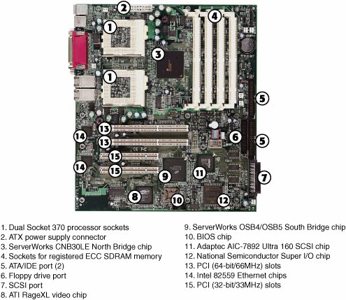
Although server chipsets typically have many features not found in desktop chipsets, they also lack some features that are common to most desktop chipsets. For example, audio and advanced video/graphics features are not necessary on servers, and thus it's not surprising that most server chipsets lack support for onboard audio, don't support AGP or PCI-Express video cards, and might not support Microsoft's gaming API, DirectX (which is the case with some ServerWorks chipsets). Although server motherboards often support integrated SCSI and PCI or low-end AGP video, these features are not native to a server's chipset but are provided by discrete chips from other vendors. (See Figure 3.1, later in this chapter, for a typical example of a motherboard with onboard SCSI and VGA support.) Figure 3.1. A typical dual Socket 370 (Pentium III) server motherboard, showing component locations. The North Bridge and South Bridge ArchitecturesMost of Intel's earlier chipsets (and, until recently, virtually all non-Intel chipsets) are broken into a multitiered architecture incorporating the North Bridge and South Bridge components, as well as a Super I/O chip:
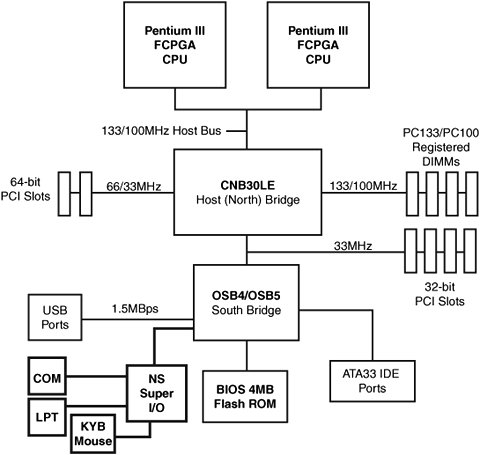
Figure 3.1 shows a typical dual Socket 370 motherboard using North Bridge/South Bridge architecture, the ServerWorks Super P3TDL3, with the locations of all major chips and components identified. The North Bridge is sometimes referred to as the PAC (PCI/AGP controller). It is essentially the main component of the motherboard and is the only motherboard circuit besides the processor that normally runs at full motherboard (processor bus) speed. Most modern chipsets use a single-chip North Bridge; however, some of the older chipsets actually consist of up to three individual chips to make up the complete North Bridge circuit. The South Bridge is the lower-speed component in the chipset and has always been a single individual chip. The South Bridge is a somewhat interchangeable component in that different North Bridge chips are often designed to use the same South Bridge component. This modular design of the chipset allows for lower cost and greater flexibility for motherboard manufacturers. Similarly, many vendors produce several versions of pin-compatible South Bridge chips with different features to enable more flexible and lower-cost manufacturing and design. The South Bridge connects to the 33MHz PCI bus and contains the interface or bridge to the 8MHz ISA bus (if present). It also typically contains dual ATA/IDE hard disk controller interfaces, one or more USB interfaces, and, in later designs, even the CMOS RAM and real-time clock functions. In older designs, the South Bridge contained all the components that make up the ISA bus, including the interrupt and DMA controllers. The third motherboard component, the Super I/O chip, is connected to the 8MHz ISA bus or the low-pin-count (LPC) bus and contains all the legacy ports that are built in to a motherboard. For example, most Super I/O chips contain the serial ports, parallel port, floppy controller, and keyboard/mouse interface. Optionally, they might contain the CMOS RAM/clock, IDE controllers, and game port interface as well. Systems that integrate IEEE 1394 and SCSI ports use separate chips for these port types, as in Figure 3.1. Most recent motherboards that use North Bridge/South Bridge chipset designs incorporate a Super-South Bridge, which incorporates the South Bridge and Super I/O functions into a single chip. Additional features, such as the onboard SCSI and VGA video found on the motherboard shown in Figure 3.1, are provided by third-party chips. Although SCSI chips used on server motherboards usually support high-performance SCSI (Ultra160 or Ultra320) and might also support SCSI RAID arrays, VGA video support is usually at a minimal level. For example, the ATI Rage XL video chip used in the motherboard shown in Figure 3.1 supports only 8MB of video memory and lacks advanced 3D graphics performance. Because a server's video is typically used only for monitoring and diagnostics, advanced features are not needed. Figure 3.2 illustrates the block diagram of the motherboard shown in Figure 3.1. Note that the 33MHz 32-bit PCI bus is used as the connection between North and South Bridge chips as well as for expansion slots. Also, USB 1.1 ports on this system are used only for low-speed (1.5MBps) input devices, such as keyboards and mouse devices. Figure 3.2. The North Bridge/South Bridge architecture used by the motherboard shown in Figure 3.1. Intel Hub ArchitectureThe newer 8xx, 9xx, 72xx, 73xx, 85xx, and the E75xx series server chipsets from Intel use hub architectures in which the former North Bridge chip is now called a MCH and the former South Bridge is called an ICH. Rather than being connected through the PCI bus, as in a standard North Bridge/South Bridge design, they are connected via a dedicated hub interface that is much faster than PCI. Hub architectures offer a couple advantages over traditional North Bridge/South Bridge designs:
The MCH interfaces between the high-speed processor bus (1066/800/533/400MHz) and video buses such as AGP (up to 533MHz) or PCI-Express x8 (2GBps) or x16 (4GBps), if present. Some systems connect a PCI-X hub (133MHz) to the PCI-Express x8 bus. The ICH interfaces between the ATA (IDE) ports (66/100MHz), the SATA ports (150MBps or faster), and the PCI bus (33MHz). If PCI-Express x1 slots (250MBps) are present, they are usually interfaced via the ICH. Some systems also connect PCI-X slots (100/133MHz) to the ICH. The ICH also includes an LPC bus, consisting basically of a stripped 4-bit-wide version of PCI designed primarily to support the motherboard ROM BIOS and Super I/O chips. By using the same 4 signals for data, address, and command functions, only 9 other signals are necessary to implement the bus, for a total of only 13 signals. This dramatically reduces the number of traces connecting the ROM BIOS chip and Super I/O chips in a system as compared to the 98 ISA bus signals necessary for older North Bridge/South Bridge chipsets that used ISA as the interface to those devices. The LPC bus has a maximum bandwidth of 16.67MBps, which is much faster than ISA and more than enough to support devices such as ROM BIOS and Super I/O chips. Intel server chipsets for Pentium 4, Xeon, and Itanium use two different versions of hub architecture:
HI 1.5 supports a 266MBps connection between the MCH and ICH chips, while DMI supports a 1MBps connection in each direction. HI 1.5 is an updated version of Intel's original Accelerated Hub Architecture (AHA) that was introduced with its first 8xx-series chipsets for Pentium III processors. Table 3.2 cross-references the hub architectures and Intel server chipsets that use a particular hub architecture.
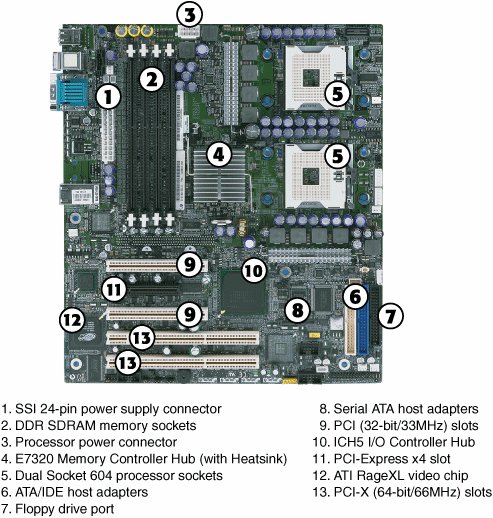
Figure 3.3 shows a typical Intel server motherboard that uses hub architecturethe SE7320SP2. Figure 3.3. A typical dual Socket 6040 (Xeon) server motherboard, showing component locations. Figure 3.4 illustrates the block diagram of the motherboard shown in Figure 3.4. When you compare this to Figure 3.2, note that the PCI and PCI-X buses are connected to the ICH. Figure 3.4. The hub architecture used by the motherboard shown in Figure 3.3.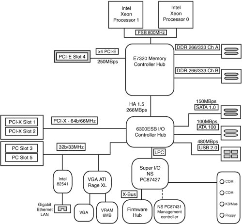 VIA V-LinkV-Link is bus technology that VIA Technologies created to compete with Intel's Hub Architecture. VIA Technologies designed the V-Link architecture to connect its North Bridge and South Bridge chips at speeds matching or exceeding those of Intel Hub Architecture, using a dedicated 8-bit data bus. It is currently implemented in three versions:
All VIA South Bridge chips in the VT82xx series support V-Link. The first chipsets to use V-Link were VIA's 266-series chipsets for the Pentium III, Pentium 4, and Athlon processor families. VIA's newer chipsets also use V-Link. Although VIA is best known as a desktop and portable chipset vendor, some of its chipsets are used in Athlon-based server motherboards made by various companies. The ServerWorks Inter Module Bus (IMB)Most recent ServerWorks chipsets for Intel server processors use a unique high-performance interconnect between the North Bridge and the 64-bit PCI bridge. This interconnect, known as the Inter Module Bus (IMB), is a high-speed serialized data bus. The speed of IMB varies with the chipset, as shown in Table 3.3.
The Champion models' thin IMB performance of 1GBps is sufficient to support Pentium III Xeon processors, which feature 100/133MHz FSB and PC100/133 registered memory. However, the faster performance of Xeon processors, which are based on the Pentium 4 design, demands faster connections. The GC-SL and GC-LE Grand Champion chipsets support Xeon processors with 400MHz or 533MHz FSB connections. The GC-LE's greater memory bandwidth is preferable for use with systems that use multiple 64-bit PCI cards. The GC-HE Grand Champion supports up to four processors, compared to up to two for other Grand Champion models. However, because these processors have FSB speeds of only 400MHz, 4.8GBps of memory bandwidth is adequate to support their operation.
HyperTransportAMD's Opteron and other 64-bit AMD processors (Athlon 64, Athlon 64 X2, Turion, and Socket 754 Sempron) use HyperTransport as their interconnection between the processor and the chipset. HyperTransport is also used by most chipsets for these processors as the interconnect between chipset components. Although HyperTransport is sometimes referred to as "AMD HyperTransport," its original developer, AMD, released HyperTransport to the HyperTransport Consortium (www.hypertransport.org) in 2001. Besides AMD, other founding members include Sun Microsystems, Apple Computer, Broadcom (the parent company of ServerWorks), Cisco Systems, NVIDIA, and Transmeta. The consortium now manages and develops HyperTransport interface technology for use in server and PC chipsets, processors, and other technologies. How HyperTransport WorksHyperTransport uses low-voltage differential signaling (LVDS) over high-speed connections of varying widths to perform low-latency transfers. HyperTransport is a full-duplex interconnect technology, supporting simultaneous two-way connections between chips. HyperTransport supports asymmetrical connections to provide appropriate bandwidth for different applications. For example, an Opteron processor uses a 16-bit-wide Side A HyperTransport connection to a HyperTransport bridge chip that supports PCI, PCI-X, or PCI-Express connections. However, the bridge chip might use an 8-bit-wide Side B HyperTransport connection to the HyperTransport hub that supports USB and other slower ports. Note Connections to the host are known as Side A connections. Connections to the next chip in the chipset are known as Side B connections. HyperTransport speeds are rated in megatransfers (MT) per second. Tunnels, Bridges, and HubsChips used between the host (processor) and the hub (equivalent to South Bridge) are known as tunnel chips because they pass HyperTransport signals through to the next device. A tunnel chip can provide a direct connection to a device, such as the AMD-8151 AGP 3.0 graphics tunnel, or it can provide bridges (interconnects) to bus types such as PCI, PCI-X, and PCI-Express. HyperTransport devices use independent data streams to carry traffic between the host, tunnel chips, and the hub. When a chip receives a data stream, it determines whether it is the intended target; if it is not, it passes the data stream to the next chip. Figure 3.5 shows the block diagram for a typical server configuration using components of the AMD-8000 chipset. Note that the AMD-8000 does not include a North Bridge. That is because the AMD Opteron processor contains its own memory controller rather than relying on a memory controller in the chipset. Figure 3.5. A typical implementation of HyperTransport on a server using an AMD Opteron processor.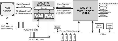 Four-Way and Eight-Way Server ChipsetsAlthough chipsets designed for single-processor and dual-processor servers are similar in many ways to desktop chipsets, the greater complexity of four-way and eight-way servers that use Intel processors requires the use of more specialized chips than the multipurpose North Bridge/South Bridge or MCH and ICH designs used for single-processor or two-way servers. A chipset designed for a four-way or eight-way server typically uses several chips to interface and control memory instead of a traditional North Bridge, and it might use specialized chips to provide PCI expansion slot support instead of or along with a traditional South Bridge.
|
EAN: 2147483647
Pages: 240