7.12 Digital Video Interfacing Chipsets
| | ||
| | ||
| | ||
7.12 Digital Video Interfacing Chipsets
Implementation of digital video systems is much easier now that specialized chips are available. The introduction of HD-SDI has required significant increase in chip performance to support the additional bit rate. HD chips are thus more expensive than their SD equivalent. One useful move is that HD and SD chips are being made with the same pinouts. Thus a single circuit board can be made into an SD or an HD device just by installing chips of the appropriate speed.
Figure 7.30 shows a hypothetical 4:2:2 component system starting with analog signals and ending with the same to illustrate the processes which are necessary. The syncs on Y are separated and multiplied in a phaselocked loop to produce a 27MHz master clock. This is divided by 2 and by 4 to produce the sampling clocks for the convertors. This results in three data streams, which can be multiplexed to form a parallel interface signal using a parallel encoder chip such as the Sony CXD8068G. This parallel signal may be output using a set of ECL line drivers. If it is required to convert the parallel signal to SDI, a serial encoder will be required. The Sony SBX1610A and the Gennum GS9002 contain all parallel-to-serial functions, but output logic level signals which require a CXA 1389AQ or a GS9007 cable driver to produce the 1.6 volt pk-pk SDI signal which will fall to the standard 0.8 volts after passing through the source terminating resistors.
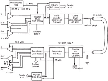
Figure 7.30: A hypothetical 422 system showing applications of various digital interfacing chips.
At the receiving end of the cable the signal requires equalization, clock regeneration and deserializing. The Sony SBX1602A provides all of these functions in one device whereas the Gennum solution is to combine equalization and reclocking in the GS9005 and to perform deserialization in the GS9000. In both cases the output is parallel single-ended data which can be returned to the parallel interface specification using ECL drivers. Alternatively the parallel data may be sent directly to a parallel interface decoder such as the Sony CXD8069G which demultiplexes the 27 MHz data to provide separate outputs for driving three DACs.
Figure 7.31 shows a block diagram of the CXD8068G parallel interface encoder. This accepts the parallel input from three component ADCs and multiplexes them to the 27 MHz parallel standard. The rounding process allows ten-bit inputs to be rounded to shorter word lengths. The limiter prevents out-of-range analog signals from producing all-ones or all-zeros codes which are reserved for synchronizing. In addition to a 27 MHz clock derived from horizontal sync, the chip requires horizontal and frame drives to operate the timing counters which address the TRS generator. The final multiplexer selects TRS patterns, video data or ancillary data for the ten-bit parallel output.
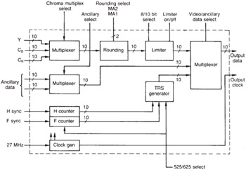
Figure 7.31: The three data streams from component ADCs can be multiplexed into the parallel interface format with the encoder chip shown here.
Figure 7.32(a) shows the SBX1601A serial encoder and (b) shows the GS9002 serial encoder. Of necessity these chips contain virtually identical processing. Parallel input data are clocked into the input latch by the parallel word clock which is multiplied in frequency by a factor of ten in a phase-locked loop to provide a serial bit clock. There is provision for selecting several centre frequencies for composite or component applications. The data latch output is examined by logic that detects input sync patterns and extends eight-bit sync values to ten bits. The parallel data are then serialized in a shift register prior to passing through the scrambler and the transition generator.
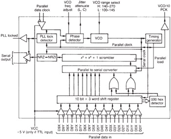
Figure 7.32a: An SDI encoder chip from Sony. See text for details.
Figure 7.33 shows an SDI cable driver chip. The device shown has quadruple outputs and is useful in applications such as distribution amplifiers . Note that each differential amplifier produces a pair of separate SDI outputs. The fact that these are mutually inverted is irrelevant as the SDI signal is not polarity conscious. Note the resistor networks that provide correct cable source termination.
Figure 7.34(a) shows the Gennum GS9005 reclocking receiver. This contains an automatic cable equalizer and a phase-locked loop clock recovery circuit that drives a slicer/sampler to recover the channel waveform to a logic level signal for subsequent descrambling in a separate device. The equalizer operates by estimating the cable length from the input amplitude and driving a voltage-controlled filter from the signal strength. A buffered eye pattern test point is provided. The equalizer output is DC restored prior to slicing to ensure that the slicing takes place around the waveform centre line. The slicer output will contain timing jitter and so a phase-locked loop is used having a loop filter to reject the jitter. The jitter-free clock is used to drive the data latch which samples the slicer output between transitions. The VCO centre frequency can be selected from four values and provision is made for an adjusting potentiometer for each frequency.
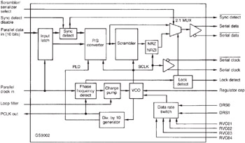
Figure 7.32b: An SDI encoder chip from Gennum. See text for details.
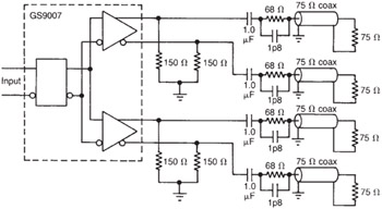
Figure 7.33: SDI cable driver chip provides correct 0.8 V signal level after source termination resistors.
Figure 7.34(b) shows the GS9000 serial decoder which complements the GS9005. This contains a descrambler and a serial-to-parallel convertor synchronized by the detection of TRS in the shift register. The chip also contains an automatic standard detector that outputs a two-bit standard code for external indication and to select the centre frequency of the GS9005. The single-ended parallel output can be converted to the differential parallel output standard using a multiple ECL driver such as a VS621.
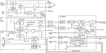
Figure 7.34: (a) Reclocking SDI receiver contains a cable equalizer and is an important building block for SDI routers as well as being the fast stage of an SDI decoder. Decoder is shown in (b). Note auto standard sensing outputs which can select VCO frequency in the reclocker.
Figure 7.35 shows the Sony SBX1602A, which contains all of the serial receiving functions in one device. Its operation should be self-evident from the description of the Gennum devices above.
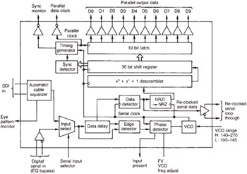
Figure 7.35: Sony SDI receiver chip for comparison with Figure 7.34.
Parallel data can be demultiplexed for conversion to analog by the CXD8069G device shown in Figure 7.36 that also extracts ancillary data. The TRS detector identifies sync patterns and uses them to direct the ID word to the Hamming code error-correction stage. This outputs corrected timing signals that are decoded to produce analog video timing drives. A FIFO (First in First out) buffer acts as a small timebase corrector to allow the DACs to be driven with a stable clock. Ten-bit video data may be rounded to shorter word lengths if required, prior to demultiplexing into separate component outputs.
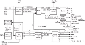
Figure 7.36: This device demultiplexes component data to drive separate DACs for each component as well as stripping out ancillary data.
As the HD protocol is based heavily on the SD protocol, HD chipsets differ primarily in the bit rate they can handle. Detail differences include the generation of the line count parameter and CRC following SAV and the need for a different sync recognition system owing to the interleaving of two TRS codes in the serial bitstream. Figure 7.37 shows a typical HD serial system.
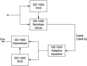
Figure 7.37: Components of a typical HD-SDI system.
| | ||
| | ||
| | ||
EAN: 2147483647
Pages: 120