2.4 Verification
Today about 70 percent of design cost and effort is spent on verification. Verification teams are often almost twice as large as the RTL designers at companies developing ICs. Traditionally, chip design verification focuses on simulation and regression. However, new verification techniques are emerging. Figure 2.7 shows several types of design verification and validation, which are also described here.
Figure 2.7. Types of Design Validation and Verification
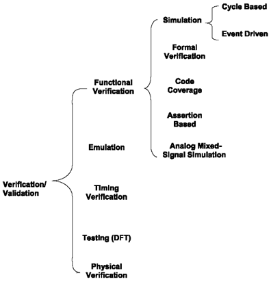
Functional Verification
Functional verification is an important part of design validation. Functional verification must be done at all levels of hierarchy in the design. It must be done at both chip and block levels.
Simulation
Simulation techniques are used at both RT and gate levels. Depending on the size of the design entity and the simulation run time, the RTL designers choose between cycle-based (where all nodes are evaluated at the cycle boundaries) and / or event-driven (where all nodes are evaluated at every event) simulators.
Testbenches
Testbenches can be categorized into the following three major categories:
-
Vector-based. This is the traditional way of writing testbenches where the stimulus and the response are in the form of vectors.
-
BFM-based. The bus functional model-based test benches are easier to write sequences for and can be reused. However, it is hard to predict the device response.
-
C-based. This is a high-performance algorithm execution that uses C-language constructs. However, C is not designed for hardware verification.
Testbench creation and automation tools are becoming very popular among design and verification engineers . Two examples are Vera from Synopsys and Specman Elite from Verisity.
Formal Verification
Formal verification is a mathematical method for determining the equivalence of two representations of a circuit. It is mainly used for RTL-to-RTL, RTL-to-gate, and gate-to-gate comparisons. Formal verification doesn't use any test vectors and is much faster than conventional simulation techniques. This is an effective method of verification after insertion of test logic and clock tree into the original circuit. EDA tools from Synopsys and Verplex, Inc., are examples of formal verification tools.
Code Coverage
An effective way of checking RTL is code coverage. Code-coverage tools essentially check the RTL code to find out what portions have been exercised in the design. Types of coverage tests include state machine, branch, path , expression, condition, triggering, and toggle.
Assertion-Based Verification (ABV)
This traditional black-box approach to verification discovers bugs at the boundaries of the box. ABV uses a so-called white-box approach to verification. Here the user can discover internal bugs early on, before they propagate outside of the box and corrupt the rest of the system. Assertion-based verification is used at RT level for both Verilog and VHDL. ABV tools are available from Cadence Design Systems and 0-In Design Automation, Inc.
Analog Mixed-Signal (AMS) Simulation
AMS simulation deals with both analog- and digital-simulation techniques to verify a circuit. Therefore, it is more complex than either digital or analog techniques alone. The analog blocks are usually modeled and verified using predefined models of basic elements (resistor, capacitor , etc.) with SPICE simulators. Some common SPICE simulators are H-SPICE, P-SPICE, Z-SPICE. Although SPICE simulators are very accurate, they are not fast simulators. Once an analog block is verified, its interface will be dealt with as a digital interface in an SOC-integration process.
Emulation
In-circuit emulation is the process of running a software model of an ASIC with the real system. Emulation is much faster than simulation and is an attractive method for large ASICs, providing the entire design is placed in the emulation engine. However, emulation is not used for block-level verification, is expensive, and is used late in the design-verification process.
This method of design validation is not suitable for detailed design debugging.
Design for Test (DFT)
DFT is an important part of the design and validation process. DFT techniques were traditionally performed before the floorplanning step (see Figure 2.2). However, as part of the new design methodologies, DFT techniques should be considered and applied at several points in the design process. For example, scan insertion can be integrated into the synthesis and physical placement or ATPG is sometimes integrated with the routing process.
DFT is a vast topic, and there are whole books dedicated to the subject (for one example, see reference 8). Here, we offer a basic overview of DFT. Testing methods usually consist of boundary scan, ATPG, and memory testing techniques such as BIST.
The goal of boundary scan is to make sure that every node in the design is both controllable (controlling a node to a specific state from the primary inputs) and observable (observing the state of a node at the primary outputs) through testing methods.
The IEEE 1149.1 standard defines boundary scan as one with Test Access Port (TAP). This standard is also known as the JTAG standard, named for the Joint Test Action Group that initiated these standards on testing. The basic technique of boundary scan can be applied to both chips and boards . The dedicated test pins for TAP are as follows :
-
TRST (Test Rest)
-
TMS (Test Mode Select)
-
TDI (Test Data In)
-
TDO (Test Data Out)
-
TCK (Test Clock)
Using TAP port you can access the internal logic and pins of a chip. Figure 2.8 illustrates a generic device under test with scan cells inserted for every I/O pad in the device. Each scan cell is a storage element capable of data multiplexing. The cells are connected together to form a shift register that goes around the chip.
Figure 2.8. Device Under Test with Inserted Boundary Scan Cells: (a) Scan cell (b) Boundary scan
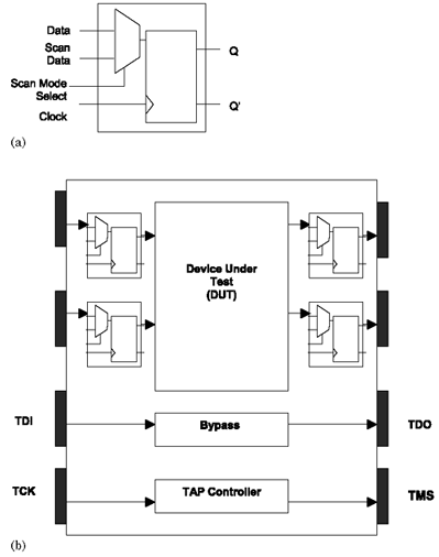
Test vectors generated by ATPG tools are applied at the scan cell inputs and the response is captured at the scan cell outputs.
Aside from being able to directly observe and control internal nodes, boundary scan is an efficient as well as an automatic testing method. However, there are few drawbacks with scan testing. These drawbacks include the following:
-
Additional time and effort are required, affecting the TAT.
-
Additional gates are required, causing an increase in the final die size. In some designs you may end up with almost 20 percent of your total logic gates dedicated to DFT logic.
-
Additional dedicated I/Os are required. This impacts package pins.
-
Elevation of the overall chip power consumption is required.
-
Negatively impacts timing.
ATPG tools generate test vectors using algorithmic methods. There are techniques available to convert RTL simulation results into files that ATPG tools can use to generate scan patterns (see reference 7 for more on this subject). ATPG tools differ from one to another depending on the algorithm they execute. Examples of these algorithms are combinational and sequential.
BIST is an effective DFT method for logic and memory elements such as RAMs and ROMs. BIST reduces the need for external testers. An ASIC can test itself once certain logic (BIST logic) is added to the chip. Similar to scan insertion, implementing BIST requires additional logic overhead.
When you meet all your DFT requirements, then the design is ready for DFT sign-off. DFT tools from LogicVision, Inc., and Mentor Graphics, Corp., are the most popular ones among chip designers.
| |
| |
| Top |
EAN: 2147483647
Pages: 61