2.2 Methodology and Design Flow
As mentioned in Chapter 1, a good design methodology consists of a set of defined design flows for both front and back end as well as for tool integration and task automation. Figure 1.7 in Chapter 1 showed the basic front-end ASIC design flow. This figure is repeated as Figure 2.2.
Figure 2.2. Front-End Design Flow (Printed with permission of Fujitsu Microelectronics America, Inc.)
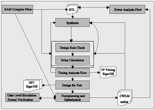
Major timing issues should be resolved here at the front end, before performing a detailed floorplan. In Chapter 4, we cover back-end or physical design flow, where you resolve minor timing issues.
Here at the front end, we start with RTL coding. This can be done in Hardware Description Languages (HDL) such as Verilog or VHDL. Lint tools should be used to check the RTL code for any coding and syntax violations. Functional simulation is the first necessary step after RTL coding is completed. Functional simulation verifies the design for its functional requirements as they are defined in the specs .
Synthesis translates a specific abstraction into the next level. For example, behavioral synthesis translates behavioral HDL to RTL architecture. Logic synthesis translates RTL into a technology-specific design in the form of gate level. Major steps in logic synthesis are translation, mapping, and optimization. The user can set his or her own constraints on area, speed, power, routability, and testability. Appropriate wire-load models (WLM), aggressive or conservative, have to be specified for the target design.
Design rule constraints must take precedence over optimization constraints because if the gates of a library cannot meet the designer's requirements, there is nothing that can be done except to get a higher performance library. The following three constraints, or specifically Design Compiler commands, should be used to ensure that the limits of the ASIC library are not exceeded:
-
set_max_fanout
-
set_max_transition
-
set_max_capacitance
Power analysis is an important part of the design process. Power-estimation as well as power-reduction techniques are done at different levels of the design abstraction, such as at RT and gate levels. We cover power analysis in Chapter 5.
The first part of timing analysis is RC extraction, which extracts parasitic information from interconnect wires. The second part is static timing analysis (STA), in which delay is calculated and timing constraints of the chip are verified . STA verifies the delays within the design. It is capable of verifying every path and can detect serious problems like glitches on the clock, violated setup and hold times, slow paths, and excessive clock skew.
DFT techniques such as scan, Automatic Test Pattern Generation (ATPG), and Built-In Self Test (BIST) are applied to the ASIC. We discuss DFT in greater detail at the end of this chapter.
Floorplanning is discussed in Chapter 4.
Some Useful Guidelines
For designs bigger than two million gates in size :
-
Use hierarchical methodology. Define sub-block boundaries and sub-block pin assignments. Use straightforward clock structure. Although clock-gating is an attractive low-power design technique, it can cause low clock skew for clock tree.
-
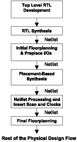
Use placement-based synthesis. This improves timing and congestion problems in the layout phase. Placement-based synthesis is applied to the pretest and preclock design. Synopsys Physical Compiler and Cadence Envisia PKS are examples of placement-based synthesis tools. Figure 2.3 shows a typical design flow with placement-based synthesis.
Figure 2.3. Design Flow with Placement-Based Synthesis
-
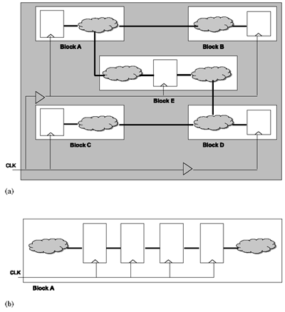
When applying hierarchical methodology, use Interface Logic Models (ILM) for Primetime timing analysis. These models improve the performance of chip-level timing analysis mainly by reducing the size of the netlist. ILMs have replaced the traditional STAMP models. Figure 2.4 shows how ILMs are used in chip-level verification. In this figure, the internal register-to-register logic is discarded for the blocks. However, I/O logic and clock tree are preserved.
Figure 2.4. (a) ILM models in Chip-Level Timing Verification (b) Inside of an ILM Model
-
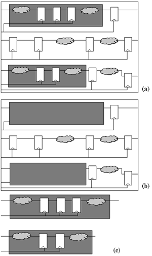
In hierarchical design methodology, three different types of timing constraints have to be defined by the logic designer (not by the physical designer). These are:
-
Chip-level timing constraints for the final timing verification.
-
Chip-level timing constraints excluding the hierarchical logic blocks (HLB). These are blocks that can be laid out independently as hard macros.
-
Timing constraints for the HLBs.
Figure 2.5 shows the three types of the timing constraints.
Figure 2.5. Timing Constraints in a Hierarchical Design (a) Chip-level analysis, (b) Chip-level analysis excluding the timing inside HLB, and (c) Timing analysis inside the HLB
-
-
Execute static timing analysis at chip-level for the following conditions:
-
System mode (min and max)
-
Test mode (min and max)
-
Key Questions for Your Design
When designing ASICs, there are a lot of issues and factors that need to be addressed early in the process. These are in addition to other well-known factors with RTL coding, logic design, timing analysis, design flow, tools, verification, and physical design issues which are covered in Chapter 4. An ASIC team should consider the following key questions:
-
What kind of system or end application is the ASIC designed for?
-
Does the chip have previous design? In the case of porting, what is the methodology for the design database migration including netlist and vector translation?
-
What is the power supply voltage? What is the tolerance level?
-
How much memory and what kinds are required? For example, what is the bit/word configuration for SRAMs? How many instances per chip? What are the speed, access time, and cycle time? How many read/write ports?
-
What will be the power consumption? Have a clear idea on the power consumption and power requirements of the ASIC you are designing; the amount of power the chip consumes affects the board and the system-level designs.
-
What is the die size estimation? The designer must perform die size estimation early on. The size of the die directly affects the power, timing, and routability and hence cost, effort, and the design schedule.
-
What is the package type? Can the package handle the required power?
-
How many high-speed signal pins does the design have?
-
What kind of interfaces are you designing for your ASIC? Is it asynchronous or source (clock) synchronous?
-
What kind of standards are you required to follow for the high-speed interface macros of your design? Examples of these standards include the following:
SFI-4 and SFI-5 from Optical Internetworking Forum
10G Ethernet for LAN, MAN, and WAN applications
IEEE802.3ae (an IEEE LAN standard)
SPI-4P2 from Network Processing Forum
| |
| Top |
EAN: 2147483647
Pages: 61