2.1 Introduction
ASICs are logic chips designed by end customers to perform a specific function for a desired application. ASIC vendors supply libraries for each technology they provide. In most cases, these libraries contain predesigned and preverified logic circuits.
Several ASIC technologies exist. These are mainly gate array, standard cell , and full custom. Some features of these ASIC technologies are summarized in Table 2.1.
See reference 3 for more details on these technologies. Typical features of ASIC devices with specific technologies that are provided by ASIC vendors are:
-
AC characteristics ” AC characteristics, or propagation delay time (t pd ), are specified for minimum, typical, and maximum values. These values are determined by wiring capacitance and resistance. Also, junction temperature, power supply voltage, and process variations are used to calculate AC characteristics.
-
DC (static) characteristics ” This data specifies the minimum, typical, and maximum values for high-level and low-level out put voltage and high-level output current as well as output short-circuit current and input leakage current. These values collectively assure the worst-case values of the DC characteristics of input and output buffers at the operating conditions.
Table 2.1. ASIC Technologies
ASIC Technology Type
Feature
Gate Array
Standard Cell
Full Custom
Complexity
Medium
Medium to Very High
High to Very High
Speed
Moderate to Fast
Fast
Fast
Development Cost
Moderate
High
High
Available I/O
High
High to Very High
High to Very High
Custom Mask Layers
Some
All
All
-
Recommended operating conditions ” These usually consist of minimum, typical, and maximum values for supply voltage, high-level input voltage, low-level input voltage, and the junction temperature. These values are recommended for normal operation of the device.
-
Power consumption ” ASIC vendors provide formulas to calculate chip power consumption. This is usually determined by the sum of power consumption of I/O buffers, internal logic gates, and on-chip memory. Tools are also available to predict power consumption of ASICs.
-
Available packages ” Examples are through-hole (dual in-line, or DIP, in both plastic and ceramic; pin grid array, or PGA, in both plastic and ceramic) and surface-mount (quad flat pack, or QFP; small outline package, or SOP; and ball grid array, or BGA). There are advantages and disadvantages with each package and the chip designer should carefully consider what package to select for the specific design.
-
Available macros ” Macros are available, ranging from basic logic gates (e.g., AND , OR , NAND , NOR , XOR ), latches and flip flops, buffers, adders, multiplexers, synchronous and asynchronous memories, to more complex cores such as CPUs, DSPs, and memory controllers.
-
Types of I/O buffers ” Selection of the appropriate input and output buffers depends on interface level, logic function, interface function, pull-up/pull-down option, and drive capability. Examples of I/O buffers are input buffers, input buffer inverting, bidirectional output buffers, and 3-state output buffers.
-
Power on/off sequence ” The sequence specifies the correct and recommended power on/off sequence for dual power supply devices as well as for internal and external power sources. Restrictions on external signal levels are also provided by ASIC vendors.
-
Analog cells ” Typical analog cells used in an ASIC device include OPAMPs, digital-analog converters (DAC), analog-digital converters (ADC), and phase locked loops (PLL).
-
PLLs ” PLLs are used for reduction of on-chip latency, synchronization of clocks between different ASICs, frequency synthesis, and clock-frequency multiplication. Refer to Appendix C for more information on PLLs.
-
Pin assignment rules ” Assignment rules for clock, clear, preset input, and simultaneous switching output pins as well as for power and ground pins are also specified by ASIC vendors.
Other technology- related information provided by the ASIC vendors for a specific ASIC technology includes the number of metal layers, the power supply for the core and the I/Os, the junction temperature, and the electrostatic discharge (ESD) specification.
In Chapter 1, we mentioned some of the factors that affect the TAT. The time it takes semiconductor vendors to make an ASIC prototype and a working part is usually referred to as the TAT, or more precisely TAT is the time taken from gate-level netlist to metal mask-ready stage. Figure 2.1 shows the degree of difficulty for TAT. The factors involved for an ASIC TAT include the following:
-
Frequency of operation
-
Number of gates
-
Density
-
Number of clock domains
-
Number of blocks and sub-blocks
Figure 2.1. Degree of Difficulty (Printed with permission of Fujitsu Microelectronics America, Inc.)
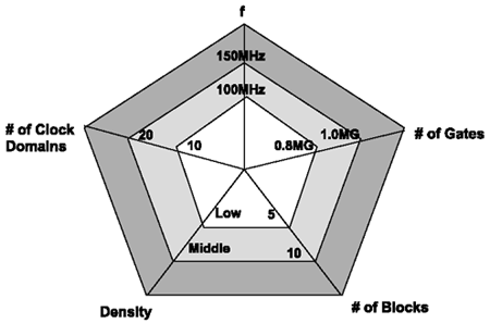
Each one of these factors directly affects the TAT. The higher the factor, the longer the TAT. The customer-vendor relationship and a clear line of responsibility also affect the TAT.
Section 2.2 covers the methodology and front-end design flow for the ASICs. Some useful guidelines are presented for the ASIC methodology. Here we assume the designers use Synopsys PrimeTime as the chip-design industry standard STA tool. Some key questions that ASIC designers must consider early on when planning for design are also covered.
In this chapter, we don't cover FPGAs. However, in Section 2.3 we discuss FPGA to ASIC conversion, which is becoming more popular among system designers for cost-cutting purposes.
An overview of the verification methodologies is covered in Section 2.4.
| |
| |
| Top |
EAN: 2147483647
Pages: 61