1.5 Design Methodology
A good design methodology for ASICs and SOCs consists of a set of defined design flows for both front and back ends as well as tool integration and task automation. Let's start with the design flow. Figure 1.4 showed a typical top-down ASIC design flow. The flow can be divided into the following major parts : design entry, design implementation, design verification, physical design, and IC production. A more detailed front-end flow diagram is shown in Figure 1.7. Let's look at the steps involved in this flow.
Figure 1.7. A Front-End ASIC Design Flow (Printed with permission of Fujitsu Microelectronics America, Inc.)
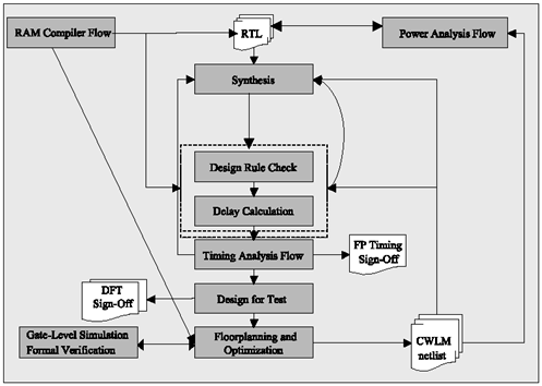
The designer develops the RTL code that implements the functional specification. Chip designers should follow any coding guidelines provided by ASIC vendors .
Simulations at the register-transfer (RT) level should be thorough because this is really the only place where correct function can be verified efficiently . Simulations at the gate level are much too slow to be complete and static timing analysis (STA) does not verify functionality, only timing.
The synthesis tool generates both forward and backward annotation files. The forward annotation provides constraints to timing-driven layout tools while the back-annotated files provide delay information to either a simulator for gate-level simulations or a static timing analyzer.
The designer is responsible for verifying the synthesized gates for functional correctness and for estimated performance. Whether the verification is done with a simulator or a static timing analyzer, the wire loads are only estimates. The gate delays come from the technology library and are accurate. The delays are provided from the synthesis tool via a standard delay format (SDF) file.
Floorplanning takes information from the synthesis step to group the cells to meet the timing performance. It feeds back more accurate wire-load models to the synthesis tool and it provides the framework for place and route.
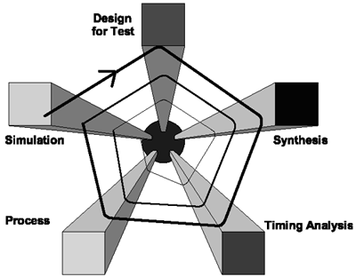
Figure 1.8 shows a spiral design flow. This type of flow is becoming popular with SOC designers for the front end. Here, the designers work simultaneously on each phase of the design until the design is gradually completed.
Figure 1.8. Spiral Design Flow
Once you finish the front-end work and generate a gate-level netlist for your design (ASIC or SOC), then you can start the physical design process.
Figure 1.9 shows a generic physical design, or back-end flow. The major steps consist of place and route, timing verification, and physical verification.
Figure 1.9. Generic Physical Design Flow (Printed with permission of Fujitsu Microelectronics America, Inc.)
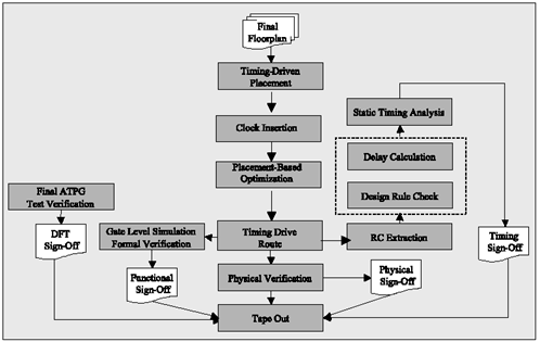
The inputs to place and route are netlist, clock definition, and I/O specification. The goal of place and route is to generate a GDSII file for tapeout. The place-and-route step performs placement, routing, clock-tree synthesis, optimization, and delay calculation.
Task automation is covered in Chapter 3.
| |
| Top |
EAN: 2147483647
Pages: 61