Up Front
| | ||
| | ||
| | ||
Before even considering burning a flash device, make sure youve made adequate preparations for the development process. The following sections discuss some preliminary measures. Many of these measures might seem obvious, but they are nevertheless important enough to mention. The tips discussed in the following sections include:
-
Get involved with the hardware design
-
Get to know the hardware and be nice to the designer
-
Have local copies of all data sheets
-
Make sure the hardware is working
-
Start slowly
-
Look at what youve created
It is also important to consider what tools you need for the development process and to ensure that the design is compatible with those tools. Several hardware-based development and debugging tools are available to assist with the embedded systems development process, including emulators, logic analyzers, JTAG and BDM interfaces, memulators, and logic probes. Many of these tools attach directly to the target device.
| |
The incircuit emulator (ICE) is a device that usually plugs into the CPUs socket on the target hardware. An emulator is designed for a specific CPU. It emulates the CPU closer than any other tool available. The emulator provides a lot of really nice features, such as an instruction trace buffer (which collects previously exe cuted instructions), complex breakpoints, and knowledge of the CPUs instruction cache. If you really need sophisticated debugging, you need an emulator.
If an emulator provides the most insight and flexibility for firmware debugging, why use anything else? This sophistication doesnt come for free. Emulators are usually quite expensive.
Because the emulator typically plugs into the same socket that normally contains the CPU, the target board must be prepared for the emulator. For example, the board designers might need to leave extra space around the CPU to accommodate the emulators sometimes bulky connector.
If you plan to use an emulator, make sure your hardware can deal with the physi cal requirements of the pod that connects the emulator with the target board. These physical access issues sometimes extend to the enclosure as well. The pod usually hangs within 12 inches of the target by some shielded multi-pin ribbon cable. So, if your target sits in a card cage and there is another card right next to it, you may be in trouble.
Because it replaces the CPU on the target, the emulator, of necessity, is quite sophisticated. Emulators are very CPU-specific, and you cannot use an emulator with a different processor without incurring substantial additional cost. Because the memory steering logic of the emulator lengthens the memory access cycle, emulators are sometimes not able to run at the full rated speed of the CPU. Also, emulators tend to become available after the CPU is already out and available, so if you are working with a bleeding-edge processor, there is a good chance the emulator will not be available when you need it.
Another problem with plugging into the socket on the target board is that the load that the emulator presents to the target system might be quite different from the load that the CPU would have put on the target. This difference in load can both mask and induce problems. In some situations, the difference in load can reduce induced noise, allowing your system to run in noisy environments until the emulator is removed. Sometimes the difference in load disturbs the target hardware, creating problems that would otherwise not be present.
Despite all of these warnings, emulators, are still very handy, and the degree to which each of these issues matters depends very much on the environment.
| |
Get Involved with the Hardware Design
First of all, make sure the boot device is conveniently reprogrammable. This point might seem obvious, but its not unusual to find systems that have the boot device soldered to the board with no reprogramming mechanism except to unsolder the device. Such a design can be painful, especially for the person writing the boot firmware. Understandably, some cost-sensitive projects must avoid sockets and other expensive components . Even so, at least one or two early versions of the board can be built with boot device sockets or a JTAG-like interface so that the boot device can be reprogrammed without the need for a soldering iron.
The design should also include some mechanism that allows the boot firmware to easily communicate with the boot firmware designer. Ideally, this communication would be via a serial port and a few LEDs. If the application is extremely cost sensitive and these extra parts are out of the question for the deliverable hardware, consider the possibility of including some expansion connector that is not populated on the final product. During development, the connector can provide additional interfaces for debugging. The only unit cost is a small increase in board size . Once again, this decision hinges on cost restrictions and other factors but providing some means of connectivity can save a lot of time in the development process.
I mentioned JTAG in the preceding section. If the CPU has some type of debug interface, then make sure that the associated pins are accessible. These interfaces become quite useful, especially if there is no other communication device tied to the processor. When the hardware is laid out, find out what JTAG-like tools are available for your CPU. Get the pinout for the tool you plan to use and make certain the hardware has a connector for it.
| |
A logic analyzer is used for general purpose logic analysis of digital hardware designs. The logic analyzer views the CPU and its address and data bus as just a collection of digital logic signals. This perspective debugging makes a logic ana lyzer useful for debugging firmware. As demand for these firmware debug tools has grown, companies that build logic analyzers have added hooks and extensions to the tools to make them look like firmware development tools. For example, with the analyzer connected to the address and data bus of the processor while the CPU is executing, the logic analyzer is collecting (and storing) the accesses . When this trace buffer is later observed by the developer, it can be viewed as a disassem bly instead of just a buffer of address bus and data bus values.
Many of the disadvantages of the emulator apply to the logic analyzer as well. Logic analyzers are usually quite expensive, they too require bulky connections (if you plan to use them for tracing instruction and data accesses), and they can introduce load into the system. An added point to keep in mind when you are using a logic analyzer for firmware debugging is that you are monitoring external, physical accesses to the address and data bus of the processor. These external transactions do not reflect data or instructions retrieved from cache. Thus, if cache is enabled, the trace buffer is really not telling the whole story. Even with the cache disabled, the user must be aware of the fact that many processors fetch blocks of instructions rather than one instruction at a time and that some of the instructions in a block might not be executed. This feature is sometimes called instruction prefetch in a processor. On the positive side, although a logic ana lyzer is rather expensive, it is an expense that can be distributed over hardware and firmware development and over several different hardware platforms, regard less of the CPU.
| |
Get to Know the Hardware and Be Nice to the Designer
Hey, Im not kidding! A good mutual friendship between the firmware and hardware folks can save a lot of frustration and time over the lifetime of a project. Let me say from experience that chances are, its not a hardware problem! A lot of small, sneaky bugs might tempt you to be suspicious of the hardware but investigate before you accuse! This advice amounts to common sense etiquette that will improve relations in any development environment.
Getting to know the hardware doesnt mean that you should look over the shoulder of the hardware designers as they are writing VHSIC Hardware Description Language (VHDL), but it certainly does help if you are familiar with at least the CPU section of the schematics. Take some time with the hardware designer and ask questions. Establish a good working relationship with the designer and the schematics. Get your own copy of the schematics and mark them up. This is important for the target hardware as well as the target CPU itself. You must also spend some time reading about the processor you are trying to tame.
| |
JTAG and BDM interfaces are becoming popular for firmware development. JTAG, or Joint Test Access Group , is a standard interface that was originally intended for hardware BIST (built-in self-test) but has been extended so that it can be used for debugging embedded systems. Background Debug Mode (BDM) is similar (implemented by Motorola) in that it is strictly dedicated to CPU- related debugging. JTAG and BDM interfaces only work with CPUs that support them, so you can't assume this option is available on every project it depends on the processor choice. The beauty of JTAG and BDM interfaces is that they usually cost less than $1,000, they are usually applicable to a processor family (not just one processor), and they require only a small, low-pin-count ribbon cable to con nect to the processor. One disadvantage of these tools is that they are very depen dent on the CPU's implementation of the interface. Another issue is that JTAG and BDM interfaces typically do not provide any kind of trace buffering capabil ity. JTAG and BDM interfaces can be used to help debug firmware, and they can also be used as a means of programming flash memory. You can usually justify a tool that costs less than $1,000 and could potentially save you a lot of develop ment legwork.
| |
Have Local Copies of all Data Sheets
You must know more than just the schematic. Each device on the schematic may come with a 200-page manual. As silicon gets denser, more and more complexity is built into the devices. It is vitally important for you, the firmware developer, to master the device behavior. In this age of electronic paper, I still find it handy to print the sections of the manual that I will be referring to the most. Printing the manual also allows you to document errors or strange behavior of a device.
This issue raises another point: make sure you check with the device vendor to see if there are any errata outstanding. It is not at all unusual to use a device that has bugs, especially if your design uses some new device from a silicon manufacturer. Worse than that, you may be the one that finds new errata. This doesnt happen often, so dont be too quick to blame the silicon, but it does happen.
Make Sure the Hardware is Working
If the hardware design is brand new and the board is fresh from the factory, make certain the designer has blessed it before you start assuming its valid. Our first run time step makes the assumption that the connection from the CPU to the flash device is correct. If youre using the board for the first time, make sure you know how to connect the power supply properly. This point may sound silly, but you sure wont get on the good side of the hardware designer if you toast the board on the first day by connecting the power incorrectly.
Start Slowly
I cant emphasize this point enough TAKE BABY STEPS!!! Dont even consider testing a large program until you have tested several small versions of the boot code. Consider the things you havent proven yet:
-
Is your program mapped to the correct memory space?
-
Do you really understand how this CPU deals with a reset/powerup?
-
Is your conversion of the executable file to binary done correctly?
-
Are you sure you configured the device programmer properly?
-
If your boot memory is wider than eight bits and it involves more than one device, are you sure you inserted the bytes into the correct device? Is the odd byte the most significant byte (MSB) or least significant byte (LSB)?
-
Does the hardware work?
A little humility here is likely to save you a lot of extra loader passes . Search the CPU manufacturers website for example boot code. In almost all cases, you will find something. Check out user groups. Do some web hunting. If possible, get some hardware assistance. If you dont know how to use an oscilloscope or logic analyzer, then get cushy with someone who does. These are priceless tools at this stage of the game.
| Note | While a logic probe is somewhat limited in capability, its convenience and price make it worth mentioning. A logic probe is an very inexpensive, hand-held instrument that allows you to read the logic level (high or low) at the probed connection. Most logic probes also support the ability to detect a clock. A logic probe is a simple pencil-like gizmo (usually with power and ground connections) that you clip onto appropriate sources. You read a pins logic level by touching the pin with the tip of this pencil. A readout (often just LEDs) on the probe will then indicate whether the pin is logical high or low, high impedance, or changing. A logic probe is very handy if you have already verified that the hardware is stable and you are just writing code to wiggle some PIO pins or a chip select. |
Look at What Youve Created
The build tools allow you to dump a memory map. See if the memory map makes sense for your target. Look at the actual S-record or binary file before you write it to the flash device. Does it make sense? Even the file size can give you a clue. If your program consists of only a very tight busy loop in assembly language, the final binary file should be very small.
Find some tool (I use elvis ) that allows you to visually display a binary file in some ASCII format. You can use this tool to confirm certain aspects of the build process. For example, to prove that flash-resident code is being placed correctly, you can modify the source to insert some easily recognized pattern at what should be the base of the flash memory (see Listing 2.8). After converting the source to binary (using the normal build process), use your dump tool to examine the file. You should find the marker pattern at the offset corresponding to the beginning for your flash memory.
| |
coldstart: .byte 0x31, 0x32, 0x33, 0x34 assembler code here
| |
Listing 2.9 is a sample dump from the elvis vi clone that displays the offset into the file, the data in ASCII-coded-hexadecimal, and the data in regular ASCII (if printable). Hence, the flash memory begins at offset 0x0000 .
| |
OFFSET ASCII_CODED_HEX_DATA ASCII_DATA 000000: 31 32 33 34 ff fd 78 14 38 60 00 30 4b fc 00 0e 1234..x.8`.0K".. 000010: 38 80 00 00 38 a0 00 00 38 c0 00 00 3c e0 00 04 8C..8a..*l..<x..
| |
The only thing you need to see in Listing 2.9 is that the first four bytes of the file are as you expected ( 0x31 , 0x32 , 0x33 , and 0x34 ).
| Note | This binary dump is also very useful if you have to split your data into separate files so you can program multiple devices that are in parallel in the hardware. Before the split, you have what is shown in Listing 2.9, and, after the split (assume a split into two files), one file is as shown in the display labeled Split A and the other file is as shown in Split B, clearly indicating that the single file was properly split. |
Split A
OFFSET ASCII_CODED_HEX_DATA ASCII_DATA 000000: 31 33 ff 78 38 00 4b 00 38 00 38 00 38 00 3c 00 13.x8.K.8.8.*.<.
Split B
OFFSET ASCII_CODED_HEX_DATA ASCII_DATA 000000: 32 34 fd 14 60 30 fc 0e 80 00 a0 00 c0 00 e0 04 24..`0".C.a.l.x.
| |
Some tools create binary files, and some tools create S-record files. As I have discussed, a raw binary file contains the exact data that is destined for the flash device, so that binary file can be transferred directly to the device programmer to be burned into the flash memory. S-records, on the other hand, are lines of text (in a file) that must be converted to the raw binary format before being written to the flash device. This conversion is usually done by the device programmer, so you would typically just transfer the S-record file to the programmer. Your toolset is likely to contain a complete description of the S-Record format, but, briefly , the format looks like this:
<S><T><LL><AAAA><DDDDDDDDDDDD><CC>
Where S denotes S-record, T is usually a value of 1, 2, or 3 indicating the size of the AAAA field. The LL field contains the length of the record; the AAAA field is a hexadecimal address that is usually 4, 6, or 8 bytes of address (16, 24, and 32 bits of address). DDDD is data to be placed at the specified address, and the final CC is a checksum of the line. Thats a nice quick summary of S-records, now the warning: If the toolset you are using builds an S-record file for your program, the result may not work without some adjustment. This is because the AAAA field that the toolset creates is relative to the CPU not the flash device. Depending on the CPU, it is very likely that the boot device does not reside at physical address 0x00000000 in CPU address space.
| |
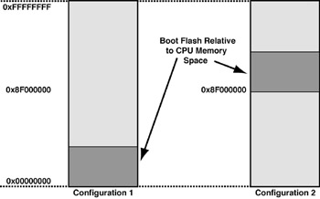
Figure 2.4: Flash Relative vs. CPU Relative Address Space.
Since memory devices usually span only a portion of the processor address space, the absolute addresses in an object format (like S-records) might need to be adjusted to be interpreted correctly by the device programmer. This requirement is because the device programmer often knows only about the memory devices address space not the processors.
Referring to Figure 2.4, in the case of Configuration 1, where the boot device resides at location zero of CPU-relative memory, the S-record CPU-relative addresses also correspond to flash device addresses, so all works well.
Configuration 2 however, does not work. Here the CPU boots from some location other than zero, so offset zero within the flash device no longer corresponds to physical address zero. Assume that this CPU boots at 0x8F000000 , so the S-record file has AAAA fields starting at 0x8F000000 because thats where the CPU sees the instructions. However, when I step away from the hardware design and go program the flash device, I must adjust the S-record address of 0x8F000000 to 0x0000000 because 0x8F000000 in CPU address space is the same as 0x00000000 in the flash devices address space. This adjustment to the S-record address can be performed in some post-processing step or in the programmer if it supports the ability to adjust the base. My personal preference is to avoid this complexity by using raw binary files instead of S-records.
| | ||
| | ||
| | ||
EAN: 2147483647
Pages: 118