10.7 Measurement types and test examples
|
10.7 Measurement types and test examples
In this section, we describe the kinds of tests that can be performed using the simple architecture of Figure 10.7. Specifically, this architecture can be programmed to perform DC curve tracing, oscilloscope, spectrum, and timing analysis functions while occupying an area equivalent to that of only a few thousand logic gates. The flexibility and compactness of such a solution makes it ideal for highly parallel testing at the block level within a complex IC or across different ICs that are tested simultaneously.
10.7.1 DC curve-tracer
DC characteristics often carry a lot of importance when characterising the large-signal behaviour of various components. Examples include the transfer characteristics of linear components and the DC linearity of A/D or D/A converters [6]. Our embedded test system can perform a DC sweep for these purposes. Specifically, the automatic waveform generator (AWG) is not limited to generating AC signals. It can be programmed to generate DC voltages using the periodic noise-shaped bit stream based generation technique described in this chapter. For each such voltage level, the DC output of the circuit under test can be digitised using our digitiser in much the same way that a voltmeter would perform a DC or RMS voltage measurement. Figure 10.19 shows such an experimental result where the DC transfer curve of a passive discrete RLC filter having a DC gain of about 0.57 V/V is measured. In this figure, the x-axis is the voltage that is encoded in our AWG, and the y-axis is the digitised DC voltage. As can be seen, the slope of the measured characteristic is about 0.57 V/V, so our test core is indeed able to extract the proper gain of the circuit.
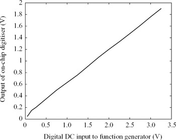
Figure 10.19: Experimental result of a DC voltage sweep applied to an external
10.7.2 Spectrum analyser
The presence of fully coherent stimulus and capture functions allows for great versatility in analogue testing. Much of the success of DSP-based techniques in reducing test time and enhancing accuracy is due to the power of coherent testing and the use of FFT techniques for frequency-domain analysis. In the proposed test core, the same versatility can be demonstrated because of the guaranteed coherence between signal sources and digitisers. To illustrate the frequency-domain capability of our test core, consider the frequency response measurement depicted in Figure 10.20. The procedure for extracting the frequency response is as follows. First, a multitone signal is encoded in a periodic bit stream. If this bit stream is fed directly to the filter under test and the filter output digitised using the on-chip digitiser, a FFT-based analysis on the digitised samples can be performed. The example in Figure 10.20 is an experimental result using the integrated prototype of Section 10.6. The figure shows an overlay of the filter magnitude response as measured by a HP3588A spectrum analyser and the result of FFT analysis on the output of our on-chip waveform digitiser (sampling at a rate of 20 Msamples/s). The filter is an eighth-order Butterworth having a bandwidth of 300 kHz. The chosen multitone frequencies were at bins 3, 11, 13, 17, and 19, where bin 1isat FS/1024. It is important to note that the spurious tones are due to quantisation noise, and they can be suppressed if a higher quantiser granularity is chosen.
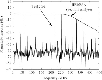
Figure 10.20: Experimental result demonstrating frequency response measurement of a lowpass filter using multitone signals. A multitone signal containing five tones was generated using our test core, and the filter response to the tones was digitised and processed
Without requiring a frequency sweep or multitone signals, other useful performance measures can be extracted using FFT-based analysis on our test system outputs. Some metrics such as SFDR, SNR, and harmonic distortion were described earlier, and they can be measured by passing only a single tone to the circuit under test and digitising its output. Figure 10.21 shows a sample experimental result of a harmonic distortion measurement. In this figure, a single tone with a peak-to-peak voltage of about 1.0 V was generated using our on-chip waveform generator. The sine wave was used to drive an external continuous-time filter, and the filter output was then digitised using our integrated prototype at a sampling rate of 20 MHz. FFT analysis was performed on the collected samples. From the figure, a total harmonic distortion of 0.19 per cent and a SFDR of about 61 dB are measured, and these numbers correlate well with an identical experiment that was performed using a HP33250A function generator with a HP3588A spectrum analyser.
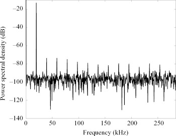
Figure 10.21: Spectral plot illustrating total harmonic distortion, SFDR, or SNR measurement
10.7.3 Oscilloscope
In normal operation, the samples at the output of our on-chip waveform digitiser can be plotted directly to give a representation of the analogue signal under test. Figure 10.22 shows an experimental example of such an operation mode, in which a single tone is simply plotted in the time domain. This figure actually consists of an overlay of two plots: the output of our arbitrary waveform generator as seen on a HP54602B digital oscilloscope, and the same signal after it was digitised using our on-chip waveform digitiser. As can be seen, the waveforms are indistinguishable. Having this ability to observe the steady-state or repetitive transient behaviour of signals internal to an IC is significant. It is not only useful for tests during production, but it is also invaluable for device characterisation or debug. Because of the complex modes of operation and the reliance on physical operating modes of active devices, analogue design is still (unfortunately) error-prone, and prototype evaluation and characterisation is an indispensable step in the process of design and manufacture. Such simple design validation capability as the one presented in Figure 10.22 can be a major aid in determining basic functionality. Many signal artefacts, such as clipping, excessive DC offset, or noise can be rapidly assessed through a simple observation of the internal time-domain waveforms.
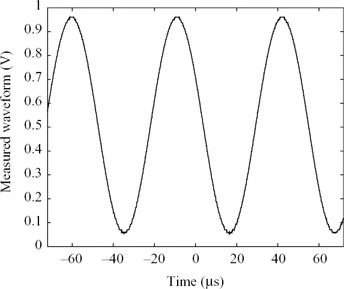
Figure 10.22: Time-domain waveform illustrating an internally digitised on-chip sine wave. This and other measurements are useful not only for production purposes, but also for debug, diagnosis and design characterisation
As was mentioned in Section 10.5, a simple modification to the comparator clocking system allows the digitiser to capture wideband phenomena without altering the overall system architecture [28]. The following examples illustrate how this subsampling mechanism is used to capture signals running at speeds equal to or more than the sampling clock. Specifically, Figure 10.23 shows a reconstructed waveform of a 25 MHz digital clock, obtained at an effective sample resolution of 1.6 GHz. The waveform is progressively reconstructed using a subsampling digitiser clock that is also running at 25 MHz [28]. The way this delayed-clock subsampling digitisation is performed is as follows. First, zero phase delay between the test core's master clock and the digitiser clock is set, and the input signal is digitised according to the algorithm described in Section 10.5. Once all the signal samples under this phase condition are digitised and stored in memory, the digitiser clock is delayed by an amount equal to 625 ps with respect to the system clock, and the input signal is again digitised. The process of incrementing the phase of the digitiser clock is repeated until the whole sampling clock period has been covered.
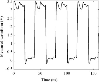
Figure 10.23: Captured rectangular waveform running at 25 MHz. Delayed-clock subsampling was used in order to achieve an effective sample rate of 1.6 GHz in a 0.35 μm CMOS process
It is interesting to note that the broadband signal being measured can also be a long pseudo-random bit sequence (PRBS), which is useful for testing GHz-rate transceiver circuits. Such a sequence can be applied to a DUT with the response of the DUT captured using the above subsampling method. In this case, an eye diagram over a unit interval can be constructed, where certain eye (signal) templates are tested to ensure an appropriate error performance rate [37]. Figure 10.24 illustrates an example of such a measurement. In this figure, the sequence being measured is slow (25 MHz), and the eye opening is artificially reduced by passing the sequence through a lowpass filter in order to emulate channel losses and inter-symbol interference in a manner similar to Reference 38.
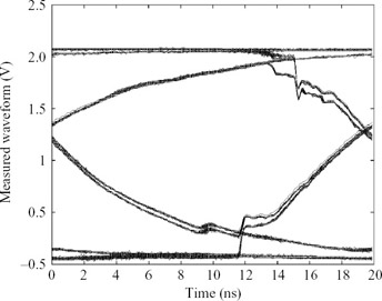
Figure 10.24: Illustration of an eye-diagram measurement. A long pseudo-random digital signal was passed through a lowpass filter to emulate a lossy channel. The output of the filter was sampled using the proposed test cores at a rate of 1.6 GHz
Before closing this section, a final useful oscilloscope function is demonstrated. Specifically, a time-domain reflectometry measurement at a sample resolution of 4 GHz is illustrated in Figures 10.25 and 10.26. Specifically, Figure 10.25 illustrates an experimental setup in which signal transmission and reflection on a piece of board interconnect is characterised using our integrated prototype. Figure 10.26 shows the actual measured result. As can be seen, a pulse was transmitted down the unterminated printed circuit board line, and the voltage at the input of the line was sampled and digitised using our integrated test core. As can be expected, time-domain measurements like this one are important in characterising the electrical characteristics of components such as packages and external interconnect discontinuities. Figure 10.26 also compares our result to that obtained by connecting the same test point to a Tektronix TDS8000 digital sampling oscilloscope using a carefully designed custom-built high-speed probe. Care was taken to ensure that the measured signal does not get altered much as it propagates through the probe and cables to the oscilloscope.
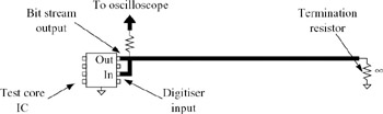
Figure 10.25: Experimental setup used to demonstrate socket/board test applications involving time-domain measurements. The probe connection to the oscilloscope was included to verify the setup
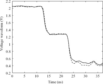
Figure 10.26: Experimental time-domain reflectometry measurement. The termination resistor in this case is an open-circuit. (-) Integrated prototype, (–) Tektronix TDS8000 digital sampling oscilloscope with 40 GHz sampling head
10.7.4 Jitter measurement device
If an edge-uncertainty or jitter measurement is sought, the above procedure to broad-band signal capture can be used, except that it is not necessary to perform a full sweep of all possible quantisation levels in each digitisation pass. Specifically, for these tests, time instance measurements are being evaluated, and these are defined by the time a signal crosses a certain fixed threshold. Thus, the comparator reference can be held to a constant level. If this is the case, noise present on the input signal being measured will alter the time this signal crosses the comparator threshold. Referring to Figure 10.27, repetitively sampling a jittery digital edge with a fixed-threshold comparator would reveal that the edge transition will occur at different times, and the variability of the transition location is going to be determined by the amount of jitter present on the signal. Since we already have a means for shifting the sampling instance of our digitiser, an application of the delayed-clock subsampling mechanism described earlier can provide information about the jitter of a signal under test. All that needs to be performed is that many such edges of the repetitive signal are obtained, and the number of occurrences of an edge at each phase delay, ΔtS, is computed. By counting the occurrence of logical highs at each of the phase delays, an edge density graph or a jitter cumulative distribution function (CDF) can be obtained [38].
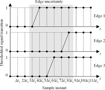
Figure 10.27: Repetitively observing the time a signal crosses a fixed threshold reveals statistical information about the underlying variability in the signal period, or jitter. Many edges have to be captured and their relative frequency of occurrence over fixed sample instances compared
An experimental result of a jitter measurement is included in Figure 10.28. In this figure, several edge transitions like the ones in Figure 10.27 are shown overlaid, one on top of the other for simplicity. The edge density graph (the count of all edge transitions at each of the sampling instants) is also illustrated in the figure. As can be seen, in this case, a peak-to-peak jitter of about 400 ps has been measured.
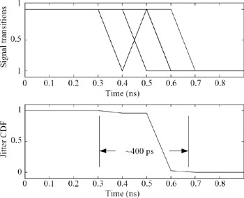
Figure 10.28: Sample jitter measurement. Edge occurrences at the different sampling instances are accumulated in order to obtain a representation of the jitter distribution function. In this example, sampling instances were spaced at 0.1 ns apart
|
EAN: 2147483647
Pages: 100