10.6 Circuit considerations and instrument performance evaluation
|
10.6 Circuit considerations and instrument performance evaluation
In this section, we delve into some of the design considerations for the analogue components of the test core described in Section 10.5 (comparator and sampler circuits). We do so in the context of an 8-bit integrated prototype that was fabricated in a 3.3 V, 0.35 μm standard CMOS process. Although many prototypes have been fabricated to demonstrate different aspects of the applicability of the proposed test core to the embedded test of analogue circuits, this prototype is sufficient to raise most of the design issues. In this section, we also present an experimental evaluation of the raw performance of the on-chip instruments in this prototype. Just like external test equipment, an evaluation of such performance capability is important. A description of how the measurement instruments are applied to sample test cases is deferred until Section 10.7.
10.6.1 Circuit considerations
The integrated prototype described here integrates all the components in Figure 10.7. Since the digital components can be automatically synthesised, and since the DC filter design can also be automated in software [32], we focus in this section on the voltage comparator and its associated S/H. A schematic of the comparator is illustrated in Figure 10.12 [34]. It consists of a preamplifier and a regenerative latch. During the track phase, the circuit behaves as a single-pole amplifier and boosts the input difference voltage slightly in order to provide a big enough seed for the latch. Once the latch signal is activated, diode-connected transistors M7/M8 are disconnected from the output nodes, and positive feedback due to cross-coupled transistors M9/M10 pushes the seed levels towards VDD or ground depending on the polarity of the comparison result. The gain of the amplifier in track mode was designed to be about 10 V/V in order to sufficiently overcome the latch offset and provide adequate amplification within a reasonable clock rate. Several comments about this comparator design should be made. First, since the input test signal is only subjected to one comparator input capacitance node, a relatively large differential pair could be used without worrying about significantly loading the driving circuitry. A large input pair means a reduced input-referred noise of the preamplifier, and hence the whole comparator. Enlarging the input pair does not threaten the implementation area since the comparator occupies only about 1.5 per cent of the overall test core area in our 0.35 μm process. Second, this comparator has the advantage of a relatively fast conversion time due to the use of both linear and non-linear amplification in the preamplifier and latch, respectively.
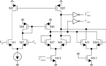
Figure 10.12: Implemented comparator consisting of a single-pole low-gain linear amplification stage followed by a positive feedback (non-linear gain) latch [34]. No offset correction was necessary for target resolution
In the comparator of Figure 10.12, we do not employ any offset compensation scheme. Thus, the common-mode dependence of offset voltage is expected to be relatively large. Such dependence would affect the linearity of the comparator and consequently the digitiser. In order to verify the viability of the comparator for the case of eight bits, a high-level MATLAB simulation of our digitisation algorithm (Figure 10.9) was performed, in which the common-mode dependence of the comparator offset was modelled. The conclusion drawn was that even an overly pessimistic signal-dependent offset variation was insignificant for the case of eight bits, so no offset cancellation was employed. This hypothesis has been verified experimentally as will be demonstrated shortly. It should also be noted that this discussion is a classic illustration of the design trade-offs involved in the implementation of the proposed test cores. The comparator is the only critical analogue component, and it should be kept as simple as could be for a given performance level. Fortunately, comparator design is governed by a small set of parameters when compared to other analogue building blocks, so its performance can be rapidly evaluated using high-level models.
An S/H circuit was placed in front of the comparator in order to provide a higher tracking bandwidth. Figure 10.13 shows a basic S/H topology that is expected to achieve very high-speed operation. When the switch (with on-resistance, Ron)is turned on, the effective bandwidth of this circuit is dependent on RonChold, which could be made quite small. Complementary switch dimensions of ~ 50 the minimum width and a 300 fF hold capacitor achieve a bandwidth of about 4.5 GHz in a 0.35 μm CMOS technology. The variation of the on-resistance of the sampling switch is a major distortion mechanism at high frequencies, and it was minimised through careful sizing of the PMOS and NMOS devices. The only remaining consideration was to ensure that the clock is slow enough so that the first-order exponential settling transient has arrived to within the required amplitude resolution.
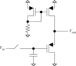
Figure 10.13: Implemented sample-and-hold amplifier. Tracking bandwidth is determined by the RC time constant of the switch on-resistance and the sampling capacitor
In order to combat the non-linearity of the S/H stage and to compensate for the signal-dependent charge injection (CI) of the switch, another replica of the S/H stage is placed at the negative comparator terminal. The reason is that we are only interested in the difference voltage across the two comparator inputs. The polarity of this difference voltage should not be affected by variations in the S/H stage characteristic, as long as the latter is monotonic and as long as the two paths are properly matched. It has been suggested [35] that matching of up to 10 bits is possible with a topology that is very similar to the one adopted in this design.
10.6.2 Experimental evaluation
This section describes an evaluation of the on-chip instruments themselves. Thus, both the stimulus and digitisation functions of the prototype IC were evaluated by connecting the appropriate instruments to known calibrated external test equipment. For example, in order to evaluate the performance of the arbitrary waveform generator, several kinds of signals were generated and observed on bench instruments such as the HP3588A spectrum analyser. Here we show only one example of a bandpass signal in Figure 10.14. In this figure, a sine wave with a frequency of about 12 MHz is encoded in a periodic ΣΔ stream running at a clock frequency, FS, of 250 MHz. The measured spectrum before filtering is shown in this figure, and the spectrum after (external) filtering using a passive filter is shown in Figure 10.15. As can be seen, with proper buffering and probing techniques, the encoded signal was extracted without significant degradation, even as the output samples were being updated at 4 ns intervals. It is interesting to note that the sine wave could have just as easily been placed at, say, 120 MHz with similar spectral purity. The reason is that spectral degradation is mainly due to the finite rise-time effects of the digital pulses, which are the same for a given clock frequency regardless of the location of the signal band.
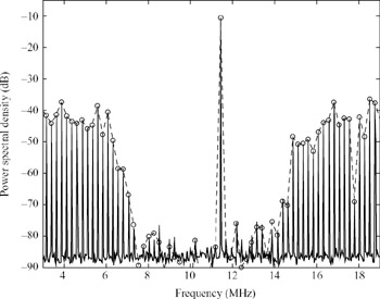
Figure 10.14: Measured spectrum of a ΣΔ modulated stream at 250 MHz as seen on a HP3588A spectrum analyser. The dashed curve is an envelope of actual programmed frequency bin power in the software. Very few spurious tones (i.e. deviations from this envelope) are apparent in the measured result
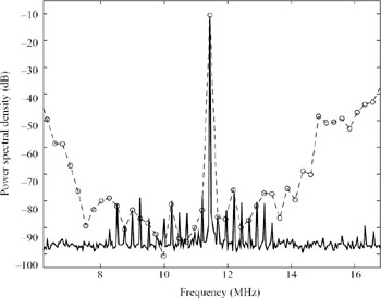
Figure 10.15: Measured spectrum of a ΣΔ stream at 250 MHz as seen on a HP3588A spectrum analyser. Filtering is performed externally using a discrete bandpass filter. The dashed curve is programmed tone power in software. Few spurious tones are apparent in the measured result
The arbitrary waveform generator was then used to verify the performance of the integrated waveform digitiser. A single tone at the fundamental frequency of the system (FS/1024) was generated at approximately 20 kHz (FS = 20 MHz). This tone was fed directly to the digitiser, and the FFT of the digitised waveform is shown in Figure 10.16. In this and all subsequent results, it was ensured that spurs due to the AC source were well below the target performance level of the digitiser. A SFDR of more than 65 dB is achieved, which is consistent with the software predicted performance of the device.
Figure 10.16: FFT-based spectral estimate of a digitised sine wave that is generated using the on-chip arbitrary waveform generator
Higher-frequency tests were performed in order to evaluate the viability of the test core for these frequencies. Although the AC bit stream generator was demonstrated to generate high-frequency bandpass signals, we did not have flexible high-frequency filtering capability with variable centre frequency to accommodate our bandpass ΣΔ modulated streams. An external RF source, an Agilent 83712B 20 GHz synthesised CW generator, was used instead. The AC bit stream generator was used to generate a 10 MHz digital synchronisation signal to which the CW generator locked on to. Synchronisation is achieved this way since our on-chip digitiser is driven by the same clock as that of the bit stream generator. Figure 10.17 shows the spectrum and reconstructed waveform of a 20.001 MHz signal that is digitised using our test core at a rate of 20 MHz. As can be seen, a SFDR of about 61 dB is still achieved at this frequency.
Figure 10.17: Sample result for a sine wave at 20.001 MHz digitised at a 20 MHz clock rate. (a) Power spectral density, (b) time-domain plot
Input stimuli at 200 MHz and higher were also digitised at a 20 MHz clock (always offset by 1 kHz), and the results are included in Figure 10.18. It should be noted that for these frequencies, an external resistor for wideband matching was placed at close proximity to the integrated prototype (which was housed in a ceramic flat pack surface-mount package capable of passing 4.5 GHz signals through short package leads) and connected to the source through a 50 Ω trace and cable. The degradation in linearity at these frequencies is attributed to clock jitter in our experimental setup. Specifically, the synchronisation signal travels through a long path from the chip to the CW generator, and it is thus corrupted by jitter. Since the generator is synchronised to this jittery signal, this will directly translate into spurious tones at its output. Despite these challenges, however, the results included in Figure 10.18 are almost on par with the best reported results in the literature on data converters targeting test applications and implemented in a similar technology [36]. Table 10.1 summarises the area and performance specifications of our integrated prototype.
Figure 10.18: Digitiser performance as a function of test signal frequency. The observed performance is similar to some of the best published data converter performance in the same technology [36]
| Technology | 3.3 V, 3 Metal, 0.35 μm CMOS |
| Amplitude resolution | 8 |
| Frequency resolution | 10 |
| Sampling rate | 20 MHz (4 GHz effective) |
| Area | 7K 2-input standard cell NAND gates (0.67 mm2) |
| Analogue area, excluding DC RC area[*] | 2.1% of Total (0.014 mm2) |
| Analogue area, including DC RC area[*] | 9% of Total (0.06 mm2) |
| Maximum DNL/INL (@ 4 MHz digitiser clock) | 0.15/0.4 |
| SFDR @ Fin = 20.001 MHz | 61 dB |
| THD @ Fin = 20.001 MHz | <0.15% |
| SFDR @ Fin = 200.001 MHz | 45 dB |
| THD @ Fin = 200.001 MHz | 0.7% |
| Maximum timing resolution | 80 ps |
| Timing system RMS (P-P) jitter[**] | 27 ps (264 ps) |
| | |
|
[*]Area does not include AC filter, which could be part of the circuit under test
[**]Limited by experimental setup [28] | |
|
EAN: 2147483647
Pages: 100