57.
4.2 Beyond Simple Logic Gates
Chapters 2 and 3 concentrated on the design of combinational logic functions with simple gates. PALs and PLAs are an IC package-efficient method for designing with simple gates.In this section we go beyond simple gates, concentrating on how to make use of higher-level, more complex logic building blocks. The idea is to do more work, that is, compute a more complex function, without increasing the number of connections to the outside world. Such logic components are often called medium-scale integration or MSI. A typical MSI component implements a function that would require from 10 to 100 discrete gates to do the same thing. If you can use these components as general-purpose logic building blocks, you can usually achieve an implementation with a smaller package count. As examples of these kinds of components, we will examine multiplexer/selector functions and decoder/demultiplexer functions.
We will also look at two classes of building blocks that do not behave exactly like logic gates. The function of the first class of components cannot always be described easily as logic equations. We tend to think about them in terms of switching networks. Examples of these kinds of circuits include CMOS transmission gates and read-only memories
(ROMs).The second class are unlike simple gates because they have output values that are different from 0 and 1. These are tri-state and open collector gates. We begin by looking at transistor switches in more detail.
4.2.1 Switch and Steering Logic
Section B.4 in Appendix B describes the basic electrical behavior of MOS transistors and how they can be combined to form standard logic gates. In this subsection, we examine alternative ways to implement logic functions as networks of CMOS switching elements, based on CMOS transmission gates.Switching networks provide an alternative to discrete gates for constructing digital systems. They operate by steering or directing inputs to outputs through a network of switching paths rather than by computing a Boolean function. You have actually seen this before in Chapter 2. The switching networks for standard gates like NAND and NOR route 0 or 1 to the output under the control of the data inputs.
For general-purpose switching networks, the primitive component is the CMOS transmission gate. It is constructed from a normally open switch
(nMOS transistor) wired in parallel with a normally closed switch (pMOS transistor), with complementary control signals. Figure 4.14 shows the switch, transistor, and schematic representations of the transmission gate. A transmission gate is equally good at passing a 0 or 1 when an external control signal is asserted. 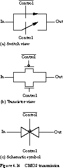
Transmission gates are not equivalent in function to any of the logic gates you have encountered so far. They are not available to TTL logic designers, only to those designing directly in CMOS technologies.
So why bother with transmission gates? They are of interest because some important digital functions can be implemented in many fewer transistors if we use transmission gates. These are usually functions that can be recast in terms of steering networks, such as shifters (more on these in Chapter 7) and multiplexer/demultiplexer circuits, which we will tackle in Section 4.2.2.
CMOS Transmission Gate Transmission gates provide an efficient way to build steering logic. Steering logic circuits are circuits that route data inputs to outputs based on the settings of control signals. As an example of such a circuit, consider the following. The circuit has two data inputs, I0 and I1, a single output Z, and a control input S. The function steers I0 to Z when S is 0 and I1 to Z when S is 1.
We call this a selector function or a multiplexer. It operates just like a switch in a railroad yard. Two independent pieces of track have to be merged into a single track. In a similar way, we often need to merge signal paths in digital logic.
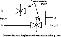
Steering logic implements the selector as shown in Figure 4.15. When S is asserted, the lower transmission gate conducts and the upper gate does not. Thus I1 is gated to Z. When S becomes unasserted, the upper transmission gate conducts and the lower gate breaks the connection. Thus, I0 is steered to Z. This multiplexer or selector function will be described in greater detail in the next subsection.
We make two observations about steering logic. First, for any combinations of the control inputs, there must be at least one conducting path from an input to the output. In other words, the output node should always be driven from some input. It should not be left floating. Second, there should never be more than one conducting path between the inputs and an output. If more than one path could exist, one of the paths might attempt to drive the output node to logic 1 while another drives it to logic 0. The resulting conflict would yield neither a logic 1 nor a logic 0 at the output node.
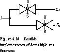
We give a second example of steering logic in Figure 4.16. This network steers its single input to Z1 if S is asserted and Z0 when S is unasserted. This function is called a demultiplexer because it performs the reverse operation of a multiplexer. Multiplexers and demultiplexers are used to implement multiple connections between components, as shown in Figure 4.16.
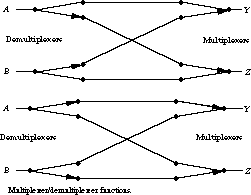
The figure shows connection paths between A and Z and B and Y. When the control settings are changed, the paths connect A to Y and B to Z. Once again, the structure looks just like the switches in a railroad yard.
There is one problem in the circuit of Figure 4.16. It violates one of our conditions for a properly functioning network. When S is asserted, I is steered to Z1, but what value is placed on the output Z0? Unfortunately, the output Z0 is neither 0 nor 1, but floats. The same problem exists for Z1 when S is unasserted. A solution with the correct behavior is given in Figure 4.16.
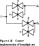
When the input steers to Z1, an additional transmission gate steers a 0 to Z0. We do something similar for output Z1 when the input steers to Z0.
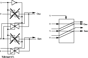
A Complex Steering Logic Example We are now ready to look at a more complex design example of what steering logic can do. Let's examine a function called the Tally circuit. A Tally circuit has N inputs (I1, I2, , In) and N + 1 outputs (Zero, One, , N). The circuit counts the number of its inputs that are at logic 1. Only one of the outputs is asserted at any time: if none of the inputs are 1, the output Zero is asserted; if one is 1, then the output One is asserted, and so on.
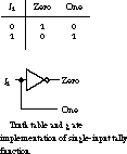
Figure 4.19 gives the truth table and gate-level implementation for a single-input Tally function. It has the single input I1 and the two outputs Zero and One. The truth table makes it clear that Zero is simply the complement of I1 and One is identical to I1.
How would we implement this function with steering logic? Remember that steering logic is good at routing inputs to outputs under the direction of control signals, so we must rethink the definition of the Tally circuit in these terms. While it may seem counterintuitive at first, in steering logic it is quite acceptable to use data signals to control transmission gates.
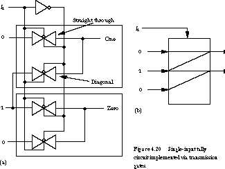
Figure 4.20(a) shows the switch network for a single-input Tally function implemented from transmission gates. The inputs are 0 and 1, I1 is used as a control signal, and the outputs are labeled Zero and One. Each output is connected to two transmission gates controlled by complementary signals. This guarantees that the network is well formed: it is not possible for both transmission gates to be conducting at the same time if their control signals are complementary.
We'll call the upper of these the "straight-through" transmission gate, and the lower the "diagonal" transmission gate. Depending on the setting of the control signals, the inputs can be steered straight through the network or can be shifted diagonally. The steering paths can be seen more clearly in the block diagram of Figure 4.20(b).
When I1 is unasserted, the straight-through gates are conducting and the diagonal gates are not. Thus, the input 0 steers to the output One while 1 steers to Zero. This is shown in Figure 4.21.
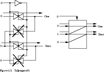
When I1 is asserted, the opposite is the case. The straight-through gates are nonconducting while the diagonal gates conduct. This causes a 1 to be steered to the One output and a 0 to the Zero output. This is shown in Figure 4.22.
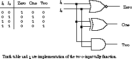
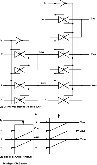
The transmission gate implementation is significantly more complex than the simple gate implementation, so it offers no real advantage. However, it does become more attractive when we have a larger number of inputs. Let's turn our attention to a two-input Tally circuit. The truth table and logic gate implementation are given in Figure 4.23.
The transmission gate implementation builds on the design of the single-input case for the two-input circuit. In essence, we decompose a two-input Tally circuit into two cascaded single-input networks. The inputs to the second stage are the Zero and One outputs from the first stage. The transmission gate implementation is given in Figure 4.24(a). Figure 4.24(b) gives its block diagram representation.
The four different cases of the two inputs and the resulting paths through the switching network are shown in Figure 4.25. Figure 4.25(a) shows what happens when both inputs are 0. The straight-through gates are enabled, setting the Zero output to 1 and the One and Two outputs to 0.
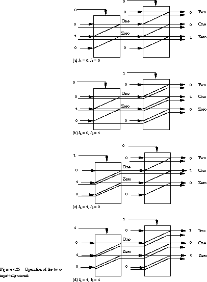
Figure 4.25(b) shows the situation when I1 is 0 and I2 is 1. The first stage passes through while the second stage shifts diagonally. The intermediate One and Zero signals are set to 0 and 1, respectively, and these are shifted up by the second stage. The second stage's One output is asserted while the Two and Zero outputs are 0.
Figure 4.25(c) illustrates what happens when I1 is 1 and I2 is 0. The network behaves symmetrically. The One and Zero intermediate outputs read 1 and 0, respectively; these are passed directly through by the second stage.
The final case is shown in Figure 4.25(d), when both inputs are 1. All of the diagonal transmission gates are enabled. The One and Zero outputs at the first stage are driven to 1 and 0, respectively. These are shifted once again by the second stage, yielding 1, 0, 0 on the Two, One, and Zero outputs.
The transmission gate implementation still looks more complicated than the approach using discrete gates. But which method is more transistor efficient? The switching network makes use of 2 inverters and 10 transmission gates: a total of 24 transistors. The gate method actually uses 26 transistors! Here is how we counted them. The two-input NOR gate is implemented with four transistors. We assume that the AND gate is implemented with an inverter and a two-input NAND gate, for six more transistors. The XOR gate actually consists of four interconnected two-input NAND gates. That's 16 more transistors. The total is 26. Thus, the switching network makes use of fewer transistors than the gate network to implement the same function. The advantage would be even more pronounced for a three- or four-input Tally circuit.
4.2.2 Multiplexers/Selectors
We next examine two very important kinds of digital building blocks. They are very much in the spirit of steering logic just described. A multiplexer/selector chooses one of many inputs to steer to its single output under the direction of its control inputs. If the input to a circuit can come from several places, a multiplexer is one possible way to funnel the multiple sources selectively to a single input. In contrast, a demultiplexer takes its single data input and steers it to one of its many outputs under the direction of its control inputs. This is a useful building block for distributing an output to one of several different nodes, as long as only one of those is to be driven at any time.More formally, a multiplexer, or mux, is a combinational logic network with 2n data inputs, n control inputs, and one data output. Depending on the settings of the control inputs, a single data input is selected and steered to the output. The 0's and 1's on the control inputs form the binary index of the input that is to be connected to the output. Because a multiplexer does nothing more than select an input for connection to the output, the terms multiplexer and selector are used interchangeably.
A demultiplexer, or demux, steers its one data input to exactly one of its many outputs. This is the reverse of the multiplexer. Decoder is another name for the component. We use the latter term when the data input is considered to be a special signal used to enable one of many similar components. This is useful, for example, in a memory system to enable one of several memory chips to place its contents on shared data wires.
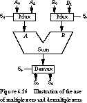
Figure 4.26 shows how these components could be used in a simple adder subsystem. There are two sources for each of the adder's inputs A and B and two destinations for the resulting sum. The control input Sa chooses between the inputs A0 and A1, while Sb selects between B0 and B1. For example, to add A0 to B1, we would set Sa = 0 and Sb = 1. By placing the appropriate signal on Ss, the sum can be connected to one of the output nodes S0 or S1.
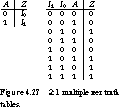
General Concept Figure 4.27 gives a "functional" truth table on the left and a more conventional truth table on the right for a multiplexer with two data inputs, I0 and I1, and one control input, A. Both communicate the same information, but the functional truth table is much easier to write down. It really communicates the idea that we are passing a selected input to the output, independent of the value of that input. Restated as a Boolean equation, the two-input multiplexer can be described as![]()
If A is left unasserted, the output is driven by I0. If A is asserted, I1 is steered to the output.
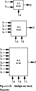
Multiplexers are described by the number of data inputs, since you can infer the number of control inputs from this. Thus, a 2:1 multiplexer has two data inputs, one data output, and one control input, while a 4:1 multiplexer has four data inputs, one output, and two control inputs. Figure 4.28 contains block diagrams for 2:1, 4:1, and 8:1 multiplexers. The Boolean equations for the 4:1 and 8:1 multiplexers generalize from the equation for the 2:1 multiplexer:
The most general expression for the multiplexer, based on the minterm form of Chapter 2, is
Alternative Implementations As we saw in the previous subsection, there are two ways to implement a 2:1 multiplexer function: logic gates or transmission gates. These alternatives generalize for functions with larger numbers of inputs.
The Boolean equations give us guidelines for the logic gate implementation.
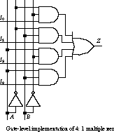
Figure 4.29 has the gate schematic for the 4:1 multiplexer. The circuit requires four 3-input gates (one for each data input), one 4-input gate, and two inverters (one for each control input), a total of seven discrete gates. Assuming these are implemented in CMOS logic, the circuit requires 36 transistors (6 transistors for each of four 3-input gates, 8 transistors for the 4-input gate, and 2 transistors for each of the two inverters). An 8:1 multiplexer requires eight 4-input gates, one 8-input gate, and three inverters (86 transistors). In standard gate libraries, such as the TTL catalog, the largest multiplexer is limited to 16 inputs. This is due in part to packaging limitations (we need 16 data pins, 4 control pins, 1 output pin, and power and ground, a total of 23 pins) and in part to limited fan-ins of the internal circuitry (16-input OR gates are hard to find because of electrical problems due to high fan-ins).
Contrast this with the transmission gate implementation of Figure 4.30.

When the control inputs A and B are both at 0, the transmission gates in the first row conduct and I0 is steered to the output Z. The transmission gate in the second row controlled by A and the gate in the third row controlled by B are also conducting, but no complete path is established between an input and Z. If A is 0 and B is 1, the second row of transmission gates is turned on, steering I1 to Z. Other transmission gates are also conducting, but there is just one completed path from the inputs to the output. When A is 1 and B is 0, the path through the third row of gates is conducting, and when both control inputs are 1, the conducting path to the output weaves through the fourth row. For the 4:1 multiplexer, only eight transmission gates and two inverters are needed, a total of 20 transistors. For functions like the multiplexer, trans-mission gates provide a more transistor-efficient implementation than discrete gates.
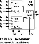
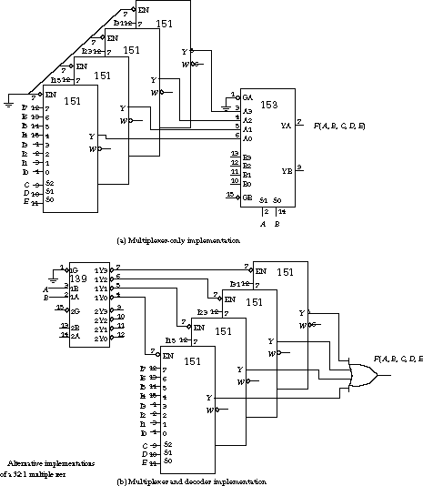
It is possible to construct an N:1 multiplexer from several multiplexers with fewer inputs. Figure 4.31 shows an implementation of an 8:1 multiplexer from two 4:1 and one 2:1 multiplexers. The first stage selects one input from the range I0 through I3 and one from I4 through I7 using the control inputs B and C. The second-stage multiplexer selects which first stage output should be gated to the final output using control input A.
This is not the only way to construct an 8:1 multiplexer, as Figure 4.32 shows.
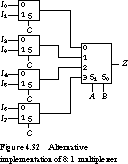
It makes use of four 2:1 multiplexers and one 4:1 multiplexer. Control signal C chooses among the even or odd inputs of the 2:1 multiplexers. The remaining control signals, A and B, choose among the outputs of the first-level multiplexers.
Even if the component library limits you to multiplexers with a restricted number of inputs, these techniques can be used to build complex multiplexers from more primitive multiplexer building blocks.
Multiplexer as a Logic Building Block Multiplexers certainly provide a useful function for implementing signal selection, but we have not yet shown how a multiplexer implements a general-purpose logic building block. In fact, a multiplexer is one way to implement a truth table directly in hardware. A multiplexer is sometimes called a hardware look-up table.
Consider the function F(A,B,C) = m0 + m2 + m6 + m7. We can implement it directly by an 8:1 multiplexer as shown in Figure 4.33.
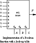
The input variables A, B, and C are connected to the multiplexer selection inputs. We simply wire Ii to 1 if the function includes minterm mi. All other inputs are set to 0. For the example, I0, I2, I6, and I7 are set to 1, while I1, I3, I4, and I5 are set to 0.
To see how this works, let's consider the case A = B = C = 0. This corresponds to the minterm m0. Given these selection inputs, the multiplexer will select I0 and F is set to 1. If A = B = 0 and C = 1, then I1 is selected and F is set to 0. This continues for all other combinations of the inputs.

We can get by with an even less complex multiplexer to implement this function. We can use two of the variables, say A and B, for the selection inputs and connect the multiplexer data inputs to 0, 1, and the third variable C or its complement.
Consider the truth table for F given in Figure 4.34. It is arranged so that F is partitioned into groups of rows that share the same values of A and B. F can then be expressed as 0, 1, or a function of C for each of the four row groups defined by the values of A and B. This is equivalent to rewriting F as![]()
We can now implement F with a 4:1 multiplexer, as shown in Figure 4.36.
The strategy presented here is easy to generalize. By selecting n - 1 variables as control inputs to a 2n - 1-input multiplexer, we can implement any Boolean function of n variables. Each choice of values for the n - 1 variables selects exactly two rows of the truth table. The two truth table rows have exactly one of the four possible values, as shown in Figure 4.36.
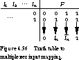
If the truth table rows are both 0 or both 1, the input is the constant 0 or 1, respectively. Otherwise the truth table rows correspond to the variable or its complement, and the input should be wired to the variable or its complement, respectively.
(A,B,C,D) whose K-map is given in Figure 4.36. 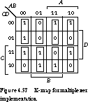
Since it is a function of four variables, it can be implemented by an eight-input multiplexer. Let's select A, B, and C as the control inputs. This immediately partitions the K-map into eight pairs of K-map entries, each sharing common values for the three control inputs. Each pair can be replaced by the appropriate function of the remaining variable D, as shown in the truth table template of Figure 4.36. In essence, we are rewriting the equation:
The multiplexer that realizes this function is shown in Figure 4.38.
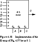
An 8:1 multiplexer is available in a single TTL package. Now let's suppose an additional inverter is needed to form the complement of D, yielding at most two packages to implement the function. Using the usual methods for forming a minimized sum of products implementation of F, we get![]()
This requires five 3-input gates and one 5-input gate plus four inverters, a total of 10 gates available in perhaps three to four TTL packages. Internally, the multiplexer may use many more gates, but in terms of TTL packages (or standard cell library elements) the use of a complex building block like the multiplexer can be more efficient.
TTL Multiplexer Components When you examine real digital component catalogs, the devices you find are slightly different from those described thus far. The catalog versions have one or more control inputs whose purpose is to enable the device for operation.
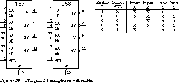
Figure 4.39 contains schematic shapes for the TTL 74157 and 74158 quad 2:1 multiplexers. The inputs and outputs of the four multiplexers are labeled with the indices 1 through 4. The inputs are A and B, and the output is Y. The four multiplexers share the same select line (SEL). SEL plays the same role as control input A in Figure 4.27. The A inputs steer to the Y outputs if SEL is 0, and the B's steer to the Y's if SEL is 1. Note that the 74158 has active low/negative logic outputs. A selected input at a logic 1 level (asserted in positive logic) will be output as a logic 0 (asserted in negative logic).
The remaining input is the signal G. This is an enable signal shared among all of the multiplexers in the package. The bubble notation tells us that the enable is active low: the device is enabled when a 0 (asserted in negative logic) is placed on G. For the 74157, a disabled device has all of its outputs driven low (unasserted in positive logic). The opposite is true for the 74158: when it is disabled, all of the outputs are driven to high (unasserted in negative logic). This behavior is summarized in the truth table of Figure 4.39.
4.2.3 Decoder/Demultiplexer
A demultiplexer is the opposite of a multiplexer: a single input is gated to exactly one of the outputs. It is also an excellent device for generating mutually exclusive signals. Consider the following design situation. We have several digital subsystems, each of which implements its own particular function. But the overall system is designed so that only one of these is to be active at any given time. Now let's suppose that each subsystem has a special "enable" signal which indicates that it has been selected to perform its function. We have seen exactly such signals in the multiplexer components just described.A demultiplexer is exactly the correct device to use in this situation. First we set the demultiplexer input to the asserted value of the enable signal. Then we drive the demultiplexer control inputs with the binary index of the output signal to be steered from the input. This signal carries the enable signal to the selected subsystem, while the remaining outputs are left unasserted. When used in this manner, the demultiplexer is often called a decoder.
General Concept A decoder/demultiplexer takes as input a single data input
(an enable signal) and n control signals and uses the latter to assert one of 2n output lines. For example, a 1:2 decoder/demultiplexer has two inputs, G (enable) and S (select), and two outputs, O0 and O1. The Boolean equations for the outputs are as follows: If G is left unasserted, both outputs are at 0. Otherwise the value of S determines which of the two outputs will be driven high. The equations for the 2:4 and 3:8 decoders are obvious generalizations.
A decoder/demultiplexer is typically named by the number of control signals and the number of output signals (for example, 1:2, 2:4, 3:8). Contrast this with the multiplexer naming: the number of data inputs and the number of data outputs (for example, 2:1, 4:1, 8:1).
Alternative Implementations
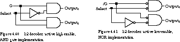
Figure 4.41 gives a gate-level implementation of a 1:2 decoder. The two inputs are G, the enable signal, and a control signal Select. When Select is unasserted, G is gated to Output0 and Output1 is driven to 0. When Select is asserted, the opposite happens: G steers to Output1 and Output0 is set to 0. If G is unasserted, both outputs are left unasserted no matter what the value of Select. We can say that the decoder has an active high enable (the selected output is a logic 1 when G is asserted in positive logic) and uses AND gates for its implementation.
This is not the only way to construct such a decoder. Figure 4.41 shows the same function implemented with NOR gates. In this case, the enable signal, ![]() , is active low. If Select is unasserted
, is active low. If Select is unasserted (logic 0/positive logic) and ![]() is asserted
is asserted (logic 0/negative logic), then Output0 is asserted in positive logic. When Select is asserted, if ![]() is also asserted, Output1 will become asserted. Once again, if
is also asserted, Output1 will become asserted. Once again, if ![]() is not asserted, both outputs are left unasserted.
is not asserted, both outputs are left unasserted.
The implementation of decoders with larger numbers of select lines and outputs generalizes from the 1:2 decoder.

Figure 4.41 gives two implementations, one with AND gates and one with NOR gates, for a 2:4 decoder. The inverters generate the four possible combinations of the two select lines: ![]() ,
, ![]() ;
; ![]() ,
, ![]() ;
; ![]() ,
, ![]() ; and
; and ![]() ,
, ![]() . For given values of the select lines only one of these combinations will be asserted. Each combination is input to one of the AND gates, along with the enable input G. When G is asserted, the output associated with the one asserted combination will be driven to 1. All other outputs will be driven to 0.
. For given values of the select lines only one of these combinations will be asserted. Each combination is input to one of the AND gates, along with the enable input G. When G is asserted, the output associated with the one asserted combination will be driven to 1. All other outputs will be driven to 0.
Note that the NOR implementation requires the complements of the select line combinations, as well as an active low enable signal ![]() . For example, in the AND implementation, the inputs to the
. For example, in the AND implementation, the inputs to the ![]() gate are
gate are ![]() ,
, ![]() , and G. In the NOR case, these become
, and G. In the NOR case, these become ![]() ,
, ![]() , and
, and ![]() .
.
As you may expect, it is also possible to implement decoder and demultiplexer logic using CMOS transmission gates. After all, a decoder simply directs the enable signal to the correct output based on the select line settings. You may have already seen this implementation in Figure 4.16. Simply substitute G for I and Select for S to have a switch implementation of the decoder.
For the 1:2 decoder, the gate implementation is less transistor efficient than the transmission switch implementation. The two NOR gates and the inverter use 10 transistors while the four transmission gates use only 8 transistors. Of course, the inverter for ![]() adds another two transistors in the second approach.
adds another two transistors in the second approach.
Now let's consider the 2:4 decoder.
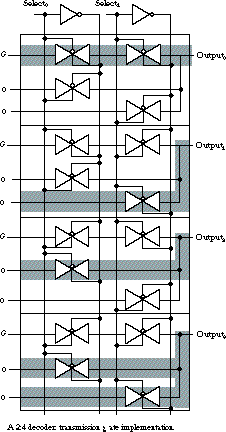
Figure 4.42 shows its transmission gate implementation. The path from G to each of the four outputs passes through two transmission gates. Each path is controlled by a different combination of the Select lines. A path is disabled if one or both of the transmission gates are not conducting. Note that each output is also connected to two parallel transmission gates whose inputs are 0. These are controlled by complementary signals to the transmission gate immediately above them. Thus, if the upper path is disrupted, one of the lower paths will conduct. This guarantees that G will be steered to the output node if the upper path conducts and will be driven to a logic 0 otherwise. The figure shows the conducting paths to the output nodes when Select0 = Select1 = 0. This implementation requires 16 transmission gates and 2 inverters, a total of 36 transistors. The discrete gate implementation, four 3-input NOR gates and two inverters, needed only 28 transistors. For this function, the transmission gate implementation is inferior to the discrete gate approach.
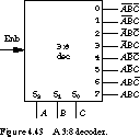
Decoder/Demultiplexer as a Logic Building Block A decoder can also be viewed as a "minterm generator." Figure 4.43 shows a block diagram of a 3:8 decoder where the select lines are labeled with the signals A, B, C. Each output can be labeled with the select line combination that causes that output to be asserted. For example, suppose the control signals A, B, and C are set to 0, 1, and 0, respectively. This corresponds to the minterm ![]() and output 2 is enabled. In other words, if the inputs correspond to minterm mi then decoder outputi will be the single asserted output.
and output 2 is enabled. In other words, if the inputs correspond to minterm mi then decoder outputi will be the single asserted output.
Although the decoder is not intended as a general-purpose combinational logic building block, it can be used in such a manner. Any function expressed in sum of products form over n variables can be implemented by an n:2n decoder in conjunction with OR gates.
To see how this can be accomplished, let's consider the following three functions of the Boolean variables A, B, C, D:
![]()
It is more convenient to reexpress the functions as
F1 is already in canonical sum of products form. To get F2 into canonical sum of products form, we expand the term ABC to two 4-variable terms: ABC![]()
+ ABCD. Finally, we represent F3 as the complement of the function ABCD, which is in the appropriate sum of products form.
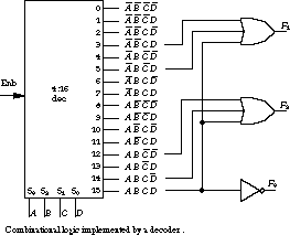
Figure 4.44 shows how to implement these functions using a 4:16 decoder. F1 is asserted whenever any of its three minterms are asserted. By connecting A, B, C, and D to the decoder select lines, the output O5 (![]() B
B![]() D
D), O3 (![]()
![]() CD
CD), or O15 (ABCD) will be asserted if the inputs correspond to the desired minterms. F1 can then be implemented by an OR gate connected to these decoder outputs. For example, if A = B = C = D = 0, the decoder output O0 is asserted and F1 is not asserted. But if A = B = C = D = 1, the decoder output O15 is asserted and now F1 is asserted.
Similarly, F2 can be implemented by a three-input OR gate connected to the decoder outputs O12 (AB![]()
![]()
), O14 (ABC![]()
), and O15 (ABCD). F3 is implemented by an inverter driven by the O15 decoder output.
This approach to implementing logic is most advantageous for functions of a relatively small number of variables (decoders of more than four select inputs are not available in a single package) and a small number of minterms per function.
TTL Decoder/Demultiplexer Components
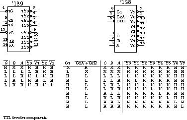
Figure 4.45 shows two TTL decoder components, the 74139 dual 2-line to 4-line decoders/demultiplexers and the 74138 3-line to 8-line decoder/demultiplexer. We begin by discussing the 74139. A close examination of the schematic indicates that the enable signal ![]() is active low, as are the decoder outputs
is active low, as are the decoder outputs ![]() through
through ![]() . This means that a disabled 74139
. This means that a disabled 74139 (the ![]() input is high
input is high) will have all of its outputs at a logic 1. When it is enabled (the ![]() input is low
input is low), exactly one of these outputs will be driven low, that is, asserted in negative logic, while the remaining outputs go high. The select inputs, A and B, determine which output is asserted: B = A = 0, Y0 is asserted; B = 0, A = 1, Y1 is asserted; B = 1, A = 0, Y2 is asserted; B = 1, A = 1, Y3 is asserted. The high-order selection bit is B and A is the low-order bit. The function is described by the truth table in Figure 4.45.
The 74138 comes with three enable inputs, G, ![]() , and
, and ![]() ; three select inputs, A, B, and C; and eight outputs
; three select inputs, A, B, and C; and eight outputs ![]() through
through ![]() . Once again, two of the enable inputs and all of the outputs are active low. The 74138 is enabled when G is at a logic 1 while both
. Once again, two of the enable inputs and all of the outputs are active low. The 74138 is enabled when G is at a logic 1 while both ![]() and
and ![]() are 0. C is the high-order selection bit, A is the low-order bit. The function is summarized by the truth table in Figure 4.45.
are 0. C is the high-order selection bit, A is the low-order bit. The function is summarized by the truth table in Figure 4.45.
We can often combine standard multiplexers and decoders to build even larger multiplexer and decoder blocks. Figure 4.46 shows two alternative methods for implementing a 32:1 multiplexer. In Figure 4.46(a), we simply select among the outputs of four 8:1 multiplexers with a 4:1 multiplexer. Alternatively, as in Figure 4.46(b), we can use a 2:4 decoder to enable one of the four 8:1 multiplexers. A disabled multiplexer will always output a 0. So the four outputs can be ORed together to obtain the multiplexer function. The active low decoder outputs match up with the active low enable signals on the multiplexers for proper bubble matching.
Just as with multiplexers, it is possible to build larger decoders by cascading smaller decoders.
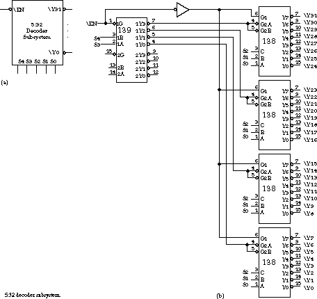
Figure 4.47 shows one possible strategy, implemented with a 2:4 decoder and four 3:8 decoders. The single active low enable signal directly enables the 2:4 decoder. It is inverted to provide the active high enable signals to the four 3:8 decoders. The active low outputs from the 2:4 decoder are wired directly to the enable signals of the second-level decoders. Only one of the 3:8 decoders is enabled, based on the selection inputs S4 and S3. And only one of this decoder's outputs will be enabled, based on the selection inputs S2, S1, and S0.
4.2.4 Tri-State Versus Open-Collector Gates
Multiplexers allow us to build circuits in which more than one signal can be gated to a particular wire under the influence of control signals. This is important, because in most technologies it is not possible to tie more than one gate to the same wire without dire results. If one gate attempts to draw the line to 0 while another actively pulls it to 1, a battle ensues in which one or both of the gates are likely to "melt down." This circuit configuration makes a relatively low-resistance path between power and ground, leading to dangerously high currents within the gates. We now examine alternatives to the multiplexer for sharing a circuit node among multiple outputs.Tri-State Outputs So far, we have seen only two possible logic values: 0 and 1. A third value we often encounter during design is the don't-care value, denoted by X. Of course, any realization of a circuit involving don't-care values in the output maps these into some assignment of 0's and 1's. So we should never encounter a don't-care value in a real -circuit.
Besides 0 and 1, we find a third signal value in digital systems: the high-impedance state, usually denoted by the symbol Z. When a gate's output is in a high-impedance state
(that is, a very high, essentially infinite, resistance exists between the power supply and ground lines and the output), it is as though the gate were disconnected from the output. Gates that can be placed in such a state are called tri-state gates: they can produce as outputs the three values 0, 1, and Z. In addition to its conventional inputs, a tri-state has one more input called output enable. When this input is unasserted, the output is in its high-impedance state and the gate is effectively disconnected from the output wire. When the output enable is asserted, the gate's output is determined by its data inputs. For example, the truth table of a tri-state buffer gate is shown in Figure 4.48.
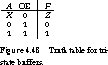
When the output enable (OE) signal is unasserted, no matter what the input is, the output will be Z. When the OE input is asserted, the buffer simply passes its input to the output.

Figure 4.49 gives a timing waveform for a buffer with a tri-state output. The input signal A changes from 0 to 1 and back between time unit 0 and 100. The OE signal is asserted between time units 25 and 75. A high-impedance output is represented by a patterned waveform, as shown in the figure. When OE is low, F is in its high-impedance state, regardless of the value of A. When OE is high, F outputs the same value as that presented at A.
Application of Tri-State Gates Let's consider the circuit fragment shown in Figure 4.50, constructed from tri-state buffers (with active high enables) and a conventional inverter.
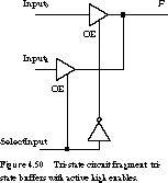
The control signal SelectInput determines which of Input0 or Input1 steers to the output node F: if Select-Input is 0 then Input0 steers to F; if it is 1 then Input1 steers to F instead.
The circuit works in the following way. A tri-state buffer passes its input to its output when the output enable signal is driven high. Otherwise, the output is high impedance (disconnected). The Input1 tri-state is controlled by SelectInput, while ![]() controls the Input0 gate. When SelectInput goes high, the Input1 tri-state is enabled and the Input0 tri-state is disabled, effectively disconnected from the output node F. When SelectInput goes low, the roles are reversed, and now the Input1 tri-state is disabled/disconnected and the Input0 tri-state drives the output node.
controls the Input0 gate. When SelectInput goes high, the Input1 tri-state is enabled and the Input0 tri-state is disabled, effectively disconnected from the output node F. When SelectInput goes low, the roles are reversed, and now the Input1 tri-state is disabled/disconnected and the Input0 tri-state drives the output node.

Figure 4.51 gives the revised circuit. This provides us with a good opportunity to test our understanding of positive and negative logic, for both data and control signals.
The tri-stated inverters now have active low output enable signals ![]() . When the active low enable signal is driven to 1, the output is high impedance, and when it is driven to 0, the output becomes the complement of the input. SelectInput is now the wrong logic polarity for enabling the Input1 tri-state: it is a positive logic control signal, but the gate expects negative logic. This is easily corrected by placing an inverter between SelectInput and the
. When the active low enable signal is driven to 1, the output is high impedance, and when it is driven to 0, the output becomes the complement of the input. SelectInput is now the wrong logic polarity for enabling the Input1 tri-state: it is a positive logic control signal, but the gate expects negative logic. This is easily corrected by placing an inverter between SelectInput and the ![]() signal for the Input1 tri-state. Now, when SelectInput is asserted in positive logic, the inverter maps it into an asserted signal in negative logic, thus enabling the tri-state buffer. The relationship between SelectInput and the Input0 tri-state's enable is complementary. If SelectInput is not asserted in positive logic, it is asserted in negative logic, and it is already in the desired form for controlling the Input0 tri-state.
signal for the Input1 tri-state. Now, when SelectInput is asserted in positive logic, the inverter maps it into an asserted signal in negative logic, thus enabling the tri-state buffer. The relationship between SelectInput and the Input0 tri-state's enable is complementary. If SelectInput is not asserted in positive logic, it is asserted in negative logic, and it is already in the desired form for controlling the Input0 tri-state.
The second complexity of Figure 4.51 is that the input data are complemented by the tri-state gate. To revert to positive logic, we can place a second-stage inverter between the tri-states and the output node F.
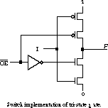
Figure 4.52 shows a switching network implementation of an inverting tri-state gate with active low enable. It looks very much like the CMOS implementation of an inverter, but with one critical difference. Switches controlled by the output enable signal and its complement isolate the output node. Let's suppose the ![]() signal is at logic 1, unasserted in negative logic. Then the pMOS transistor controlled by
signal is at logic 1, unasserted in negative logic. Then the pMOS transistor controlled by ![]() is nonconducting and the nMOS transistor controlled by its complement is also nonconducting. This leaves the output node F floating. Now let's suppose that the
is nonconducting and the nMOS transistor controlled by its complement is also nonconducting. This leaves the output node F floating. Now let's suppose that the ![]() signal is driven low, becoming asserted in negative logic. The switches controlled by
signal is driven low, becoming asserted in negative logic. The switches controlled by ![]() and its complement are now both closed and conducting. If I is a logic 1, F is connected to 0; if I is 0, then F is connected to 1.
and its complement are now both closed and conducting. If I is a logic 1, F is connected to 0; if I is 0, then F is connected to 1.
The principle of using tri-state gates to connect selectively an input to an output wire generalizes for connecting n input signals to the same output wire. For large n, this represents a considerable savings in gates.
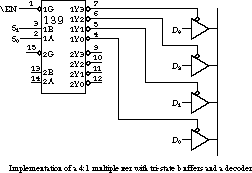
Figure 4.53 shows one way to implement a multiplexer with a decoder and tri-state gates. Based on the values of S1 and S0, only one of D3, D2, D1, or D0 will be gated through to the shared output wire.
Open-Collector Outputs There is one more way to implement multiple simultaneous connections to a single wire. The idea is to provide a gate that can only pull its output down to 0. If the output is to be 1, the voltage on the wire is left floating. To make this behave properly, the output wire must be attached to a resistor that pulls it to a logic 1 voltage if none of the connected gates are attempting to pull the wire low. The resistor is chosen to be large enough that it can be easily overcome by the pull-down resistances of any attached gates. These gates are called open-collector gates.
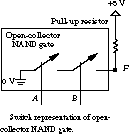
Figure 4.54 shows the switch-level circuitry for an open-collector NAND gate. The output is 0 only when A and B are both asserted. Otherwise the node F is floating. The resistor will pull it up to a logic 1 voltage.
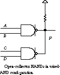
Figure 4.55 shows two open-collector NAND gates in what is called a "wired-AND" configuration. When both inputs to the NAND gate are 1, the output is low and node F is pulled low. In the other input configurations, the gate's output floats and is pulled up to 1 by the resistor.
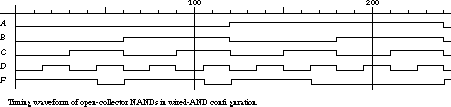
The open-collector output is active only in cases in which the NAND gate is unasserted! The configuration is called a wired-AND because the effect on F is just as though both NAND gates had been ANDed together: if either gate has an output 0 or both do (that is, both inputs to the gate are 1), then F will be at 0; only when both gates have their outputs asserted is F at a logic 1 (that is, any input combination other than both inputs at 1). This is clearly shown in the timing diagram of Figure 4.56.
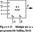
We show a possible circuit to implement a mux in Figure 4.57.
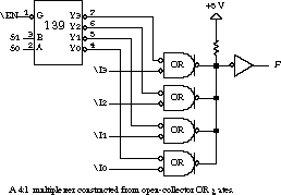
The decoder maps its two selection inputs, S1 and S0, into one of its four outputs to be asserted active low. Note that the data inputs, ![]() ,
, ![]() ,
, ![]() , and
, and ![]() , are also active low. Suppose the decoder selects the topmost OR gate
, are also active low. Suppose the decoder selects the topmost OR gate (![]() is driven to 0
is driven to 0) and ![]() is also asserted
is also asserted (active low). The OR gate pulls the shared wire low, and the inverter asserts the output F active high. If ![]() is not asserted, the shared wire stays high and the output is driven low.
is not asserted, the shared wire stays high and the output is driven low.
We can think of the wire shared by the OR gates as active low. A signal is asserted onto the wire by pulling it low. The pull-up provides an unasserted default value. It pulls the wire high if none of the OR gates pull it low. The inverter hanging off the wire restores the signal to positive logic. This is a common usage with open-collector circuit nodes: they are designed to be active low, with inverters converting the signals back to positive logic where needed.
In general, open-collector gates and tri-state gates are used for the same kinds of functions. But tri-states are more economical because they do not require the external resistor. They have largely replaced open-collector gates in modern designs.
TTL Tri-State and Open-Collector Components
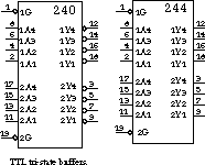
Figure 4.58 shows two different TTL tri-state buffer components. The 74240 octal buffer with three-state outputs is organized into two independent 4-bit sections, each with its own enable, data inputs, and data outputs. The enable inputs are ![]() , the data inputs are 1A1-1A4 and 2A1-2A4, and the eight data outputs are
, the data inputs are 1A1-1A4 and 2A1-2A4, and the eight data outputs are ![]() -
-![]() and
and ![]() -
-![]() . The enable signals are active low while the outputs are inverted. For example, output
. The enable signals are active low while the outputs are inverted. For example, output ![]() is high impedance when enable
is high impedance when enable ![]() is high. When
is high. When ![]() goes low,
goes low, ![]() is driven to the complement of the value on the 1A1 input.
is driven to the complement of the value on the 1A1 input.
The function of the 74244 is identical to that of the 74240, except that the outputs are not inverted. Once again, the enables are active low. A logic 1 on ![]() yields high impedance on output 1Y1. When
yields high impedance on output 1Y1. When ![]() is driven to logic 0, 1Y1 receives whatever logic value is placed on 1A1.
is driven to logic 0, 1Y1 receives whatever logic value is placed on 1A1.
Open-collector gates are available in packages similar to those of conventional discrete gates. The TTL components 7406 and 7407 contain six open-collector inverting and noninverting buffers, respectively. The 7426 and 7433 contain four 2-input NAND and NOR gates, -respectively.
4.2.5 Read-Only Memories
Perhaps the ultimate form of look-up table logic is the read-only memory, or ROM. A ROM is really nothing more than a circuit that implements a two-dimensional array of 0's and 1's. The internal storage elements of the ROM are set to their values once and after that are only read.(This is not completely true because some technologies, called EPROM or erasable programmable ROM, allow the contents to be erased and rewritten at a later time. Since the process of erasure takes minutes or even hours, you should think of any kind of ROM as something you write very infrequently and read mostly.) Each row of the array is called a word and is selected by the control inputs, which are called the address. The number of columns in the array is called the bit-width or word size. The number of words and the word sizes of commercially available ROMs are almost always powers of 2. General Concept
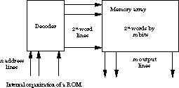
Figure 4.59 gives a block diagram view of a ROM. The ROM contains its own internal decoder that maps the address lines into word select lines. Each line selects a unique ROM word, which in turn is gated onto the output lines. As we know from our discussion of decoders, the selection lines correspond to each of the unique minterms of the variables at the address lines. This is not very different from the product terms formed by the AND array of a PAL. At least conceptually, a ROM is just like a PAL with a fully decoded AND array. There is a word line for every possible product term combination of input variables at the address lines.
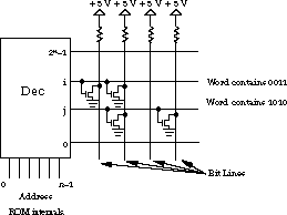
Figure 4.60 shows the ROM in more detail. The n-input address decoder asserts one of the 2n selection lines. These are also called word lines. Each vertical wire, representing an output from the ROM, is called a bit line. You can think of the bit lines as being connected to open-collector inverters. A transistor controlled by the word line pulls down the bit line if a zero is to be stored in that word. If there is no pull-down transistor for that word and bit line, a one is stored instead. Based on the placement of the pull-downs, the wordi contains the value 0011 while wordj stores 1010.
Figure 4.61(a) shows a block diagram of an 8-word by 4-bit wide ROM. A ROM is frequently used to store the truth tables of a set of functions, as in the sample ROM contents of Figure 4.61(b).
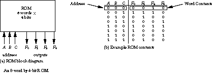
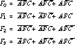
The variables over which the functions are defined, in this case A, B, and C, form the address. Depending on their values, the appropriate row of the truth table, and the corresponding ROM word, are selected. Each output function is associated with a column or bit position in the ROM. If the function is a true for that combination of inputs, a 1 is stored in the selected word at the bit position for that function. Otherwise a 0 is stored. By examining Figure 4.61(b), we get the following set of Boolean equations for the outputs:
ROMs Versus PALs/PLAs Recall Figure 4.8, which shows a truth table for a conventional circuit mapping from BCD to Gray code. To implement this as a read-only memory, we need a 4 address line (16 words) by 4-bit ROM. Each row of the truth table maps to a ROM location holding a 4-bit Gray code word, addressed by the input word in 4-bit BCD code. Don't-care entries, such as the input configurations 1010 through 1111, are of no particular advantage in reducing the hardware needed for the implementation, since the ROM comes with locations for those words whether we store 1's and 0's there or not.
Code converters are used to translate from one data representation to another. For example, a calculator uses standard binary codes for its internal calculations. But it may convert these codes into BCD for input/output and display.
Code conversions are a particularly ideal application for ROMs, since most if not all combinations of the inputs need to be generated anyway and the decoder can do this quite efficiently. So how do you choose between a ROM and a PAL/PLA-based implementation?
The answer depends on the structure of the functions being implemented. This can be quantified in terms of (1) the number of unique product terms that must be generated to implement all the output functions, (2) the degree to which these terms can be shared among multiple output functions, and (3) the number of terms that must be ORed together to implement a given output function.
PLAs are effective when the number of unique terms is small and a given term generated in the AND array can be shared among multiple outputs (this contributes to keeping down the number of unique terms). You should remember that PAL/PLA structures do not always provide enough outputs from the AND array if you need to generate many terms. And PALs are limited in the number of terms that can contribute to realizing any single output function. It will take longer to design a circuit with a PAL or PLA, since minimization methods are needed to reduce the number of terms and to maximize the number of terms that can be shared.
ROMs are effective when the number of unique terms is large. You can reduce your design time because there is no need to perform minimization: the size of the ROM is determined solely by the number of inputs and outputs, not by the number of product terms. However, the size of the ROM doubles with each additional input, so the output functions had better be of a form that requires all possible product terms if this approach is to make sense.
In the BCD to Gray code example, 10 of 16 minterms were needed, the rest being don't-cares. Boolean minimization reduced the number of literals in the terms but not the number of unique terms, which was still 10. This is a good tipoff that a ROM-based implementation is probably the best.
ROM Components ROMs come in a variety of sizes and word widths. The upper limit is represented by the 27512 EPROM, which provides 216 8-bit words, or one-half million ROM bits in a single 28-pin -package!
As an example, let's concentrate on the 2764 8192 (213) word by 8-bit ROM, whose schematic symbol is shown in Figure 4.62.
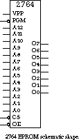
The 2764 component has 13 address lines, to identify each of the possible 8192 words, and 8 tri-state output lines, one for each bit in the ROM word. There are four additional inputs for control. The outputs are enabled by an active low output enable (![]()
) signal. The component also comes with an active low chip select input (![]()
). This can be used to cascade smaller/narrower ROMs to form larger/wider memories. We will see how this can be used in a moment. Since EPROMs are programmed by electrical pulses, an additional input places the ROM in programming mode rather than reading mode (![]()
), while the final input (VPP) provides the necessary high-voltage source used during the programming process. Outside the actual PROM programming station, these inputs are hardwired to the power supply.
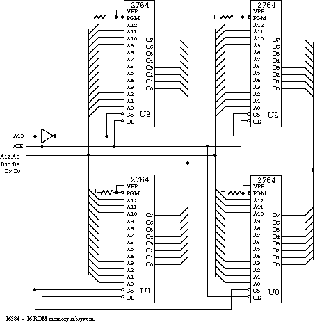
Figure 4.63 shows how the chip select lines can be used to construct a larger memory. Suppose that we are to build a memory that is 214 by 16 bits wide using the 2764 EPROM. Such a subsystem has 14 address lines (A13:A0) and 16 data lines (D15:D0). An additional ![]() signal enables the entire subsystem for output.
signal enables the entire subsystem for output.
Because this has twice the width and twice the number of words of a single 2764, we will need four of them to implement the subsystem. These components are labeled U0 through U3. The thick lines in the figure denote buses, several logically related wires that share a common function. For example, buses are used to transmit related data and address bits. This is a shorthand notation used to avoid drawing individual signal lines.
The high-order address bit, A13, selects between the higher 8192 ROM words (addresses 8192 through 16383) and the lower 8192 words (-addresses 0 through 8191). Address line A13, if low, enables U1 and U0. If high, it enables U3 and U2. The remaining address lines, A12:A0, are wired directly to the address line inputs of the ROM chips, as is the output enable signal. The output of the ROM will be driven only if the chip is -selected and the output is enabled. Because the outputs are tri-stated and the upper and lower ROM chips are never asserted at the same time, it is perfectly -acceptable to wire their outputs together. U3 and U1 are connected to D15:D8, while U2 and U0 are connected to D7:D0.
[Top] [Next] [Prev]