54.
Exercises
1.(Conversion Between Forms) Use Boolean algebra to verify the -following: The AND-OR expression of Figure 3.4 is equivalent to the NAND/NAND expression of that figure. The AND-OR expression of Figure 3.5 is equivalent to the NOR/NOR expression of that figure.
The OR/AND expression of Figure 3.6 is equivalent to the NOR/NOR expression of that figure.
The OR/AND expression of Figure 3.7 is equivalent to the NAND/NAND expression of that figure.
2.(AND-OR/NAND-NAND Mappings) Draw schematics for the following expressions, mapped into NAND-only networks. You may assume that literals and their complements are available: 3. (OR-AND/NOR-NOR Mappings) Draw schematics for the following expressions, mapped into NOR-only networks. You may assume that literals and their complements are available: 4. (Multilevel Network Mappings) Draw schematics for the following expressions, using mixed NAND and NOR gates only: 5.(Canonical Forms) Given the following function in sum of products form (not necessarily minimized):Reexpress the function in:
Canonical product of sums form. Use P M notation.
Minimized product of sums form.
in minimized product of sums form.
in minimized sum of products form.
Implement F andusing NAND gates only. You may assume that literals and their complements are available.
Implement F andusing NOR gates only. You may assume that literals and their complements are available.
Implement F andusing a single AND-OR-Invert gate. You may assume that literals and their complements are available.
Implement F andusing a single OR-AND-Invert gate. You may assume that literals and their complements are available.
6.(AND-OR-Invert Logic) Implement the following functions using AND-OR-Invert gates. Assume no limitations on inputs or the number of stacks. You may assume that literals and their complements are available. (A,B,C)=A Ý B Ý C
(A,B,C)=AB+BC+AC
(A,B,C,D)=S m(1,3,5,7,9)+S d(6,12,13)
(A,B,C,D)=P M(0,1,6,7)
(A,B,C,D)=S m(0,2,4,6)
7.(OR-AND-Invert Logic) Implement the same functions as in Exercise 3.4, but this time use OR-AND-Invert gates. Assume no -limitations on inputs or the number of stacks. You may assume that literals and their complements are available.
8.(Multilevel Logic) Factor the following sum of products -expressions: ABCD+ABDE
ACD+BC+ABE+BD
AC+ADE+BC+BDE
AD+AE+BD+BE+CD+CE+AF
ACE+ACF+ADE+ADF+BCE+BCF+BDE+BDF
9. (Multilevel Logic) Write down the function represented by the -circuit network in Figure Ex3.9 in a multilevel factored form using AND, OR, and NOT operations only-that is, no NAND or NOR operations: 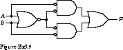
Derive the simplest Boolean expression (minimum number of -literals and fewest gates) for the function represented by this schematic. You may use any kind of logic gates described in Chapter 2.
10. (Multilevel Logic) Using Boolean algebra, K-maps, or truth tables, verify that the multilevel forms for the full adder Sum and CO (carry-out) obtained in Section 3.1 are logically equivalent to the two-level forms found in Chapter 2.
11. (Multilevel Logic) Using Boolean algebra, K-maps, or truth tables, verify that the multilevel forms for the 2-bit binary adder outputs, X, Y, and Z, of Section 3.1 are logically equivalent to the two-level forms found in Chapter 2.
12. (Multilevel Logic) Using Boolean algebra, K-maps, or truth tables, verify that the multilevel forms for the BCD increment by 1 outputs, W, X, Y, and Z, of Section 3.1 are logically equivalent to the two-level forms found in Chapter 2.
13.(Time Response) Consider the circuit in Figure Ex3.13(a).
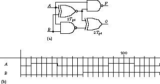
Write down its functions in minimized form. Given that XOR/XNOR gates have twice the delay of the NAND gates, what is the circuit's output response to the input waveforms in Figure Ex3.13(b)? (Each 5-time-unit division represents one NAND gate delay.)
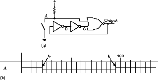
14. (Time Response) Consider the circuit with a single input in Figure Ex3.14(a). At time t0 the switch is moved to the closed (connected) position, and at time t1 the switch is returned to its original open (disconnected) position. Fill in a timing diagram showing the behavior of the internal signals B and C, and the output signal, in response to this input waveform. Assume all gates have an identical propagation delay Tpd, which corresponds to a single division on the chart in Figure Ex3.14(b).
15.(Time Response) Construct a timing diagram for the behavior of the circuit schematic in Figure Ex3.15.
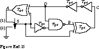
(up) as shown. Fill in the timing waveform with an initial steady-state condition for the circuit nodes labeled A, B, C, and D. Warning: It is very easy to choose an initial configuration that oscillates. A unique nonoscillating configuration does exist. Start your reasoning with the tightest loop, or make an educated guess and verify that the assumed state is indeed nonoscillating.At time T, the switch is moved from position 1 to position 2
(down). Fill in the rest of the timing diagram with the logic values of the signals at points A, B, C, and D in the given -circuit. 16.(Hazard-Free Design) Given the following specification of Boolean functions, implement them in a hazard-free manner:
F(A,B,C,D)=S m(0,4,5,6,7,9,11,13,14)

F(A,B,C,D)=P M(0,1,3,5,7,8,9,13,15)
F(A,B,C,D,E)=S m(0,1,3,4,7,11,12,15,16,17,20,28)
17.(TTL Data Book) To answer this question, you will need access to a TTL data book, preferably one published by Texas Instruments, Inc. Someone has constructed a giant 32-input AND gate from a cascaded tree of 2-input AND gates of type 74S08. This circuit is to drive an output net with 50 picofarads (pF) of capacitance. Assume that the typical capacitance of internal circuit nodes is more like 15 pF. See Figure Ex3.17. 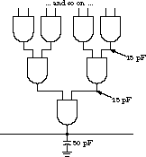
What is the typical average delay through this circuit?
What is the typical average DC power consumption of this -circuit?
18.(TTL Data Book) To answer this question, you will need access to a TTL data book. Compute the typical propagation delay and power consumption of the following TTL components:
7400 and 74S00
7402, 74S02, and 74LS02
7404, 74S04, and 74LS04
19.(TTL Data Book) To answer this question, you will need access to a TTL data book. Compute the following fan-outs: An S TTL NAND gate driving other S TTL NAND gates
An LS TTL NAND gate driving S TTL NAND gates
A standard TTL NAND gate driving LS TTL NAND gates
A standard TTL NAND gate driving S TTL NAND gates
20.(TTL Gates) It is never a good idea to allow inputs to a TTL gate to "float," that is, to be left unconnected. Give four ways to wire up the unused input of a TTL NAND gate to ensure proper operation of the gate. [Top] [Next] [Prev]