15.
1.2 Digital Hardware Systems
In this section we examine what makes digital systems different from other kinds of complex systems. We will distinguish between digital and analog electronics, briefly describe the circuit technology upon which digital hardware systems are constructed, and examine the two major kinds of digital subsystems. These are circuits without memory, called com-binational logic, and circuits with memory, known as sequential logic.1.2.1 Digital Systems
Digital systems are the preferred way to implement hardware. In this section we look at what makes the digital approach so important.
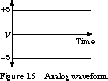
Digital Versus Analog Digital systems have inputs and outputs that are represented by discrete values. Figure 1.4 shows a digital system's typical output waveform. The X axis is time and the Y axis is the measured voltage. This system has exactly two possible output values, represented by +5 volts and -5 volts, respectively. Such systems are called binary digital systems. If you are unfamiliar with the binary number system, you should read Appendix A before continuing. Note that there is nothing intrinsic to the digital approach that limits it to just two values. The key is that the number of possible output values is finite.
In analog systems the inputs and outputs take on a continuous range of values, as shown in Figure 1.5. Analog waveforms more realistically represent quantities of the real world, such as sound and temperature. Digital waveforms only approximate these with many discrete values.
Advantages of Digital Systems The critical advantage of digital systems is their inherent ability to deal with electrical signals that have been degraded by transmission through circuits. Because of the discrete nature of the outputs, a slight variation in an input is translated into one of the correct output values. In analog circuits, a slight error at the input generates an error at the output. If analog circuits are wired together in series, the output of one feeding the input of the next, each stage adds its own small error. The sum of the errors over several stages becomes overwhelming. Digital components are considerably more accurate and reliable. They make it easier to build assemblies while guaranteeing predictable behavior.
Analog devices still play an important role in interfacing digital systems to the real world. After all, the real world operates in an analog fashion-that is, continuously. Interface circuits, such as sensors and actuators, are analog. Often you will find the two kinds of circuits mixed in real systems. The digital logic is used for algorithmic control and data manipulation, while the analog circuits are used to sense and manipulate the surrounding environment.
Binary Digital Systems The simplest form of digital system is binary, with exactly two distinct values for inputs and outputs. Binary digital sys-tems form the basis of just about all hardware systems in existence today.
The main advantage of binary systems is that the two alternative values are particularly easy to encode with physical quantities. We use the symbols 1 and 0 to stand for the two values, which can be interpreted as "yes" and "no" or "on" and "off." 1 and 0 might be physically realized by different voltage values (5 volts vs. 0 volts), magnetic polarizations (North vs. South), or the flow or lack thereof of electrical current.
Mathematical Logic Perhaps the greatest strength of digital systems is their rigorous formulation founded on mathematical logic and Boolean algebra. We will cover these topics in detail in Chapter 2, but it is useful to introduce a few basic concepts here first. Mathematical logic allows us to reason about the truth of a set of statements, each of which may be true or false. Boolean algebra is an algebraic system for manipulating logic statements.
As an example, let's look at the following logic statement:
IF the garage door is open
AND the car is running
THEN the car can be backed out of the garage
It states that the conditions-the garage is open and the car is running-must be true before the car can be backed out. If either or both are false, then the car cannot be backed out. If we determine that the conditions are valid, then mathematical logic allows us to infer that the conclusion is valid.
This example may seem remote from hardware design, but logic statements are exactly how we describe the control for a hardware system. The sequencing through the various configurations of the traffic light example of Figure 1.2 can be formulated as follows:
IF N-S is green
AND E-W is red
AND 45 seconds has expired since the last light change
THEN the N-S lights can be changed from green to yellow
The three conditions must be true before the conclusion can be valid ("change the lights from green to yellow").
It should not surprise you that statements like this are actually at the heart of digital controller design. A computer program, containing control statements like IF-THEN-ELSE, is a perfectly valid behavioral representation of a hardware system.
Boolean Algebra and Logical Operators Boolean algebra, developed in the 19th century by the mathematician George Boole, provides a simple algebraic formulation of how to combine logic values. Consisting of variables, such as X, Y, and Z, and values (or symbols) 0 and 1, Boolean algebra rigorously defines a collection of primitive logical operations, such as AND, for combining the values of Boolean variables.
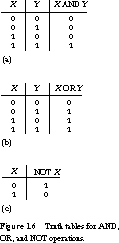
Figure 1.6(a) shows the definition of the AND function in terms of a truth table. A truth table is a listing of all possible input combinations correlated with the outputs you would see if you applied a particular set of input values to the function. Think of 0 as representing false ("no") and 1 as true ("yes"). If the variable X represents the condition of the door (0 = closed, 1 = open) and Y the running status of the car (0 = not running, 1 = running), then the truth table succinctly indicates the condition(s) under which the car can be backed out of the garage. These are exactly the input combinations that yield the value 1 for X AND Y.
OR and NOT are other Boolean operations. If either the Boolean variable X is true or the variable Y is true, then X OR Y is true (see Figure 1.6(b)). If X is true, then NOT X is false; if X is false, then NOT X is true. The truth table for this operation is shown in Figure 1.6(c).
1.2.2 The Real World: Ideal Versus Observed Behavior
So far, we have considered the ideal world of mathematical abstractions. Here we look at the real-world realities of hardware systems.Although we find it convenient to think of digital systems as having only discrete output values, when such systems are realized by real elec-tronic components, they exhibit aspects of continuous, analog behav-ior. They do so because output transitions are not instantaneous and because it is too difficult to design electronics that recognize a single voltage value as a logic 1 or 0. Digital logic must be able to deal with degraded signals. It can recognize a degraded input as a valid logic 1 or 0 and thus generate outputs at the correct voltage levels.
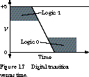
As an example, let's assume that "on" or logic 1 is represented by +5 volts. "Off" or logic 0 is represented by 0 volts. Figure 1.7 shows a signal waveform of an output switching from on/logic 1 to off/logic 0. You might observe a waveform like this on an oscilloscope trace. The transition in the figure is certainly not instantaneous. Other values besides +5 volts and 0 volts are visible, at least for an instant in time.
All electronic implementations of Boolean operations incur some de-lay. Why aren't they instantaneous? A water faucet provides a useful analogy.*
Theoretically, a water faucet is either on, with water flowing, or off, with no flow. However, if you observed the action of a faucet being shut off, you would see the stream of water change from a strong flow, to a dribbling weak flow, to a few drips, and finally to no flow at all.
The same thing happens in electrical devices. They start out by draining the output of its charge rather quickly, so that its voltage drops toward 0. But eventually the discharge slows down to a trickle and finally stops.
Voltage Ranges for Logic 1 and 0 Digital systems may seem to require a single reference voltage with which to represent logic 1 and logic 0. However, this is neither possible nor desirable. Some variation in the behavior of electrical components is unavoidable, simply because of man-u-facturing variations. Not every device will output a perfect +5 volts or 0 volts. Furthermore, a by-product of any interconnection of electrical components is noise, which causes the degradation of electrical signals as they pass through wires. Even a perfect +5 volt output signal may appear as a substantially reduced voltage farther along a wire.
The tolerance of digital devices for degraded inputs is called the noise margin. Voltages near the reference voltages are treated by the devices as though they were a perfect logic 1 or 0. A degraded input, as long as it is within the noise margin, will be mapped into an output voltage very close to the reference voltages. Cascaded digital circuits can correct signal degradations.
1.2.3 Digital Circuit Technologies
The two most popular integrated circuit technologies for the fundamental building blocks of digital(as well as analog) systems are MOS (metal-oxide-silicon) and bipolar electronics. Without going into the details, an integrated circuit technology is a particular choice of materials that either conduct, insulate, or sometimes conduct. The last are called semiconductors, and the technology usually goes by the name of semiconductor electronics. The three kinds of materials interact with each other to allow electrons to flow selectively. In this fashion, we can construct electrically controlled switches.Transistors: Electrically Controlled Switches The basic electrical switch is called a transistor. To get a feeling for how it behaves, let's examine the MOS transistor, which is perhaps the easiest to explain. We will describe MOS switches in more detail in Chapter 4.
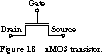
A MOS transistor is a device with three terminals: gate, source, and drain. Figure 1.8 shows the standard symbol for what is known as an nMOS (n-channel MOS) transistor. When the voltage between the gate and the source exceeds a certain threshold, the source and drain terminals are connected and electrons can flow across the transistor. We say that the switch is conducting or "closed." If this voltage is removed from the gate, the switch no longer conducts electrons and is now "open." Based on this simplified analysis, a MOS transistor is a voltage-controlled switch.
Although bipolar transistors are quite different from MOS transistors in detailed behavior, their conceptual use as switching elements to implement digital functions is very similar. We discuss bipolar transistor operation in Appendix B.
Gates: Logic Building Blocks Building upon transistor switches, we can construct logic gates that implement various logic operations, such as AND, OR, and NOT. (Logic gates are not the same as transistor gates.) Logic gates are physical devices that operate over electrical voltages rather than symbols like 1 and 0. A typical logic gate, implemented in the technologies you will study in this book, interprets voltages near 5 V as a logic 1 and those near 0 V as a logic 0.
For example, an AND gate is a circuit with two inputs and one output. It outputs a logic 1 voltage whenever it determines that both of its inputs are at a logic 1 voltage. In all other cases, it outputs a logic 0 voltage.
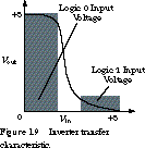
Some aspects of gate behavior are not strictly digital. Consider the inverter, implementing a function that translates 1 to 0 and 0 to 1. Figure 1.9 illustrates the inverter's output voltage as a function of input voltage. This figure is called a transfer characteristic.
Imagine that the gate's input starts at 0 volts (V), with voltage slowly increasing to +5 V. The output of the inverter holds at +5 V for some range of input values and then begins to change abruptly toward 0 V. As the input voltage continues to increase, the output slowly approaches 0 V without ever quite getting there.
The "stickiness" at a particular output voltage is what contributes to a good noise margin. Input voltages near the ideal values have the same effect as perfect logic 1 and logic 0 voltages. Any input voltage within the gray region near 0 V will result in an output voltage very close to +5 V. The same is true for the input voltages near +5 V: these yield values very close to 0 V at the output.
Gates like the inverter are readily available as preexisting modules, designed by transistor-level circuit designers. Designers who work with gates are called logic designers. By using logic gates, rather than transistors, as the most primitive modules in the design, we can hide the differences between MOS and bipolar transistors.
1.2.4 Combinational Versus Sequential Switching Networks
It is often useful for digital designers to view digital systems as networks of interconnected gates and switches. These switching networks take one or more inputs and generate one or more outputs as a function of those inputs. Switching networks come in two primitive forms. Combinational switching networks have no feedback-that is, there is no wire that is both an output and input. Sequential switching networks have some outputs that are fed back as inputs.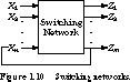
Figure 1.10 shows a "black box" switching network, with its inputs and outputs. If some of the outputs are also fed back as inputs (dashed line), the network is sequential.
Combinational Logic: Circuits Without a Memory Combinational switching networks are those whose outputs depend only on the current inputs. They are circuits without a memory. Simply stated, the outputs change a short time after the inputs change. We cover combinational logic circuits in depth in Chapters 2, 3, 4, and 5.
A switch-controlled house lamp is a simple example of a combinational circuit. The switch has two settings, on and off. When the switch is set to on, the light goes on, and when it is set to off, the light goes off. The effect of setting the switch does not depend on its previous -configuration.
Contrast this with a "three-position" lamp that can be off, on but dim, and on but bright. Turn the switch once, and the lamp is turned on dimly. Turn it again, and the lamp becomes bright. Turn it a third time, and the lamp goes off. The behavior of this lamp clearly depends on its previous configuration: it is a sequential circuit.
Another combinational network is a two-data-input binary adder, sometimes called a full adder. This circuit adds together two binary digits (also called bits) to form a single-bit output: 0 + 0 = 0, 0 + 1 = 1, 1 + 0 = 1, and 1 + 1 = 0 (with a carry of 1).
The full adder has a third input that represents the carry-in of an adjacent addition column. We also generate a carry-out to the next addition column. The bits to be added are A and B, the sum is Sum, the carry-in is Cin, and the carry-out is Cout.
The values of Sum and Cout are completely determined by the inputs. For example, if A = 1, B = 1, and Cin = 1, then Sum = 1 and Cout = 1 (that is, one plus one plus one is three in binary numbers, or 112). A block diagram of the full adder is shown in Figure 1.11.
Sequential Logic: Circuits with a Memory We discuss sequential logic circuits in Chapters 6, 7, 8, 9, and 10. In this kind of network, the outputs depend on the current inputs and the history of all previous inputs. This is a potentially daunting requirement if the system must remember the entire history of input patterns. In practice, though, arbitrary inputs lead the sequential network through a small number of unique configurations, called states.
A sequential network is a function that takes the current configuration (state) of the circuit and the inputs, and maps these into a new state with new outputs. After a delay, the new state becomes the current state, and the process of computing a new state and outputs repeats.
For our purposes, the configuration of the network changes in response to a special reference signal, the clock. This is what makes the system synchronous. There are forms of sequential circuits with no -single indication of when to change state. We call these asynchronous systems.
The traffic light controller would be implemented by a sequential switching network. Even if it has been running for years, it can be in only one of four unique states at any point in time, one for each of the unique configurations of the lights.
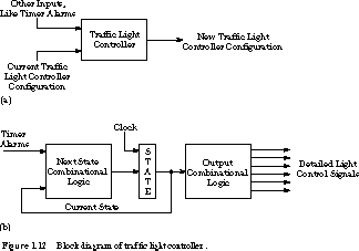
Figure 1.12(a) shows a generic block diagram of the traffic light controller's switching network. The inputs are the timer alarms and the traffic light configuration, and the outputs are the network's new configuration. Figure 1.12(b) shows the controller in more detail. It consists of two blocks of combinational logic separated by clocked logic that holds the state. Let's look at these blocks in more detail:
- The first combinational logic block, the next state logic, transforms the current state and the status of the timer alarms into the new state. The next state network contains logic to implement statements like this: IF the controller is in state N-S green/E-W red
AND the 45-second timer alarm is sounded
THEN the next state becomes N-S yellow/E-W red when the clock signal is next true - As you may guess, not all inputs are relevant in every state. If the controller is in state N-S yellow/E-W red, for example, then the next state function examines only the 15-second timer; the 45-second timer is ignored.
- The state block contains storage elements, primitive sequential networks that can either hold their current values or allow them to be replaced.
(Storage elements are described in more detail in Chapters 6 and 7.)These are loaded with a new configuration when the external clock signal ticks. You can see that the current state feeds back as input to the first combinational logic block.
- The last logic block, or output logic, translates the current state into control signals for the lights and the countdown timers. For example, on entering the new state N-S yellow/E-W red, the output logic asserts control signals to change the N-S lights from green to yellow and to commence the countdown of the 15-second timers.
This file last updated on 05/19/96 at 09:31:39.
randy@cs.Berkeley.edu;
- Linking the IT Balanced Scorecard to the Business Objectives at a Major Canadian Financial Group
- Measuring and Managing E-Business Initiatives Through the Balanced Scorecard
- Measuring ROI in E-Commerce Applications: Analysis to Action
- Governing Information Technology Through COBIT
- The Evolution of IT Governance at NB Power