13.3 The MMX Programming Environment
|
13.3 The MMX Programming Environment
The MMX architecture extends the Pentium architecture by adding the following:
-
Eight MMX registers (MM0..MM7)
-
Four MMX data types (packed bytes, packed words, packed double words, and quad words)
-
57 MMX instructions
13.3.1 The MMX Registers
The MMX architecture adds eight 64-bit registers to the Pentium. The MMX instructions refer to these registers as MM0, MM1, MM2, MM3, MM4, MM5, MM6, and MM7. These are strictly data registers; you cannot use them to hold addresses nor are they suitable for calculations involving addresses.
Although MM0..MM7 appear as separate registers in the Intel architecture, the Pentium processors alias these registers with the FPU's registers (ST0..ST7). Each of the eight MMX 64-bit registers is physically equivalent to the L.O. 64 bits of each of the FPU's registers (see Figure 13-1). The MMX registers overlay the FPU registers in much the same way that the 16-bit general purpose registers overlay the 32-bit general purpose registers.
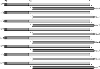
Figure 13-1: MMX and FPU Register Aliasing.
Because the MMX registers overlay the FPU registers, you cannot mix FPU and MMX instructions in the same computation sequence. You can begin executing an MMX instruction sequence at any time; however, once you execute an MMX instruction you cannot execute another FPU instruction until you execute a special MMX instruction, emms (Exit MMX Machine State). This instruction resets the FPU so you may begin a new sequence of FPU calculations. The CPU does not save the FPU state across the execution of the MMX instructions; executing emms clears all the FPU registers. Because saving the FPU state is very expensive, and the emms instruction is quite slow, it's not a good idea to frequently switch between MMX and FPU calculations. Instead, you should attempt to execute the MMX and FPU instructions at different times during your program's execution.
You're probably wondering why Intel chose to alias the MMX registers with the FPU registers. Intel, in its literature, brags constantly about what a great idea this was. You see, by aliasing the MMX registers with the FPU registers, Microsoft and other multitasking OS vendors did not have to write special code to save the MMX state when the CPU switched from one process to another. The fact that the OS automatically saved the FPU state means that the CPU would automatically save the MMX state as well. This meant that the new Pentium chips with MMX technology that Intel created were automatically compatible with Windows 95, Windows NT, and Linux without any changes to the operating system code.
Of course, those operating systems have long since been upgraded and Microsoft (and Linux developers) could have easily provided a "service pack" to handle the new registers (had Intel chosen not to alias the FPU and MMX registers). So while aliasing MMX with the FPU provided a very short-lived and temporary benefit, in retrospect Intel made a big mistake with this decision. It has obviously realized its mistake, because as it has introduced new "streaming" instructions (the floating point equivalent of the MMX instruction set), it has added new registers (XMM0..XMM7). It's too bad it doesn't fix the problem in its current CPUs (there is no technical reason why it can't create separate MMX and FPU registers at this point). Oh well, you'll just have to live with the fact that you can't execute interleaved FPU and MMX instructions.
13.3.2 The MMX Data Types
The MMX instruction set supports four different data types: an eight-byte array, a four-word array, a two -element double word array, and a quad word object. Each MMX register processes one of these four data types (see Figure 13-2).
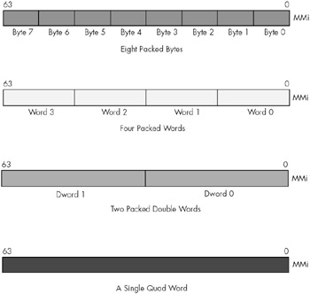
Figure 13-2: The MMX Data Types.
Despite the presence of 64-bit registers, the MMX instruction set does not extend the 32-bit Pentium processor to 64 bits. Instead, after careful study Intel added only those 64-bit instructions that were useful for multimedia operations. For example, you cannot add or subtract two 64-bit integers with the MMX instruction set. In fact, only the logical and shift operations directly manipulate 64 bits.
The MMX instruction set was not designed to provide general 64-bit capabilities to the Pentium. Instead, the MMX instruction set provides the Pentium with the capability of performing multiple 8-, 16-, or 32-bit operations simultaneously. In other words, the MMX instructions are generally SIMD (Single Instruction Multiple Data) instructions (see the electronic version of The Art of Assembly Language on the accompanying CD-ROM for details about SIMD architectures). For example, a single MMX instruction can add eight separate pairs of byte values together. This is not the same as adding two 64-bit values because the overflow from the individual bytes does not carry over into the higher order bytes. This can accelerate a program that needs to add a long string of bytes together because a single MMX instruction can do the work of eight regular Pentium instructions. This is how the MMX instruction set speeds up multimedia applications — by processing multiple data objects in parallel with a single instruction. Given the data types the MMX instruction set supports, you can process up to eight byte objects in parallel, four word objects in parallel, or two double words in parallel so the CPU should be capable of executing code up to eight times faster than without the MMX extensions.
|
EAN: 2147483647
Pages: 246