8.7 What Does This Have to Do with Computers, Anyway?
8.7 What Does This Have to Do with Computers, Anyway?
Although the connection between computer systems and Boolean logic in programming languages like C or Pascal may seem tenuous, it is actually much stronger than it first appears. There is a one-to-one relationship between the set of all Boolean functions and the set of all electronic circuits. Electrical engineers , who design CPUs and other computer- related circuits, have to be intimately familiar with this stuff.
Although the implementation of an algorithm in hardware is well beyond the scope of this book, one important point must be made with respect to such circuitry : Any algorithm you can implement in software, you can also implement directly in hardware. This means that any program you can write, you can also specify as a sequence of Boolean equations.
Of course, it is much easier to specify a solution to a programming problem using languages like Pascal, C, or even assembly language than it is to specify the solution using Boolean equations. Therefore, it is unlikely that you would ever implement an entire program using a set of state machines and other logic circuitry. Nevertheless, there are times when a hardware implementation is better. A hardware solution can be one, two, three, or more orders of magnitude faster than an equivalent software solution. Therefore, some time-critical operations may require a hardware solution.
A more interesting fact is that it is also possible to implement all hardware functions in software. This is important because many operations you would normally implement in hardware are much cheaper to implement using software on a microprocessor. Indeed, one of the primary uses of assembly language on modern systems is to inexpensively replace a complex electronic circuit. It is often possible to replace many tens or hundreds of dollars of electronic components with a single $5 microcomputer chip. The whole field of embedded systems deals with this very problem. Embedded systems are computer systems embedded in other products. For example, most microwave ovens, TV sets, video games , CD players, and other con-sumer devices contain one or more complete computer systems whose sole purpose is to replace a complex hardware design. Engineers use computers for this purpose because they are less expensive and easier to design with than traditional electronic circuitry.
You can easily design software that reads switches (input variables ) and turns on motors, LEDs, or lights, or that locks or unlocks a door. To write such software, you will need an understanding of Boolean functions and of how to implement such functions in software.
8.7.1 Correspondence Between Electronic Circuits and Boolean Functions
For any Boolean function, you can design an equivalent electronic circuit and vice versa. Because Boolean functions only use the AND, OR, and NOT Boolean operators (these are the only operators that appear within canonical forms), we can construct any electronic circuit using only these three operations. The Boolean AND, OR, and NOT functions correspond to the AND, OR, and inverter (NOT) electronic circuit gates (see Figure 8-13). These symbols are standard electronic symbols appearing in schematic diagrams . (interested readers wanted to learn more about electronic schematic diagrams should check out any book on electronic design).
Figure 8-13: AND, OR, and inverter (NOT) gates
The lines to the left of each item in Figure 8-13, with the A and B labels, correspond to a logic function input; the line leaving each diagram corresponds to the function's output.
However, you actually need only a single gate type to implement any electronic circuit. This gate is the NAND (not AND) gate, shown in Figure 8-14. The NAND gate tests its two inputs ( A and B ) and presents a false on the output pin if both inputs are true, it places true on the output pin if both inputs are not true.
Figure 8-14: The NAND gate
To prove that we can construct any Boolean function using only NAND gates, we must show how to build an inverter (NOT), an AND gate, and an OR gate. Building an inverter is easy; just connect the two inputs together (see Figure 8-15).
Figure 8-15: Inverter built from a NAND gate
Once we can build an inverter, building an AND gate is easy - just invert the output of a NAND gate. After all, NOT (NOT ( A AND B )) is equivalent to A AND B (see Figure 8-16). Of course, this takes two NAND gates to construct a single AND gate, but no one said that circuits constructed only with NAND gates would be optimal, only that they would be possible.
Figure 8-16: Constructing an AND gate from two NAND gates
The remaining gate we need to synthesize is the logical-OR gate. We can easily construct an OR gate from NAND gates by applying DeMorgan's Theorems.
(A or B)' = A' and B' DeMorgan's Theorem. A or B = (A' and B')' Invert both sides of the equation. A or B = A' nand B' Definition of NAND operation.
By applying these transformations, you get the circuit in Figure 8-17.
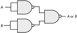
Figure 8-17: Constructing an OR gate from NAND gates
You might be wondering why we would even bother with this. After all, why not just use logical AND, OR, and inverter gates directly? There are two reasons. First, NAND gates are generally less expensive to build than other gates. Second, it is also much easier to build up complex integrated circuits from the same basic building blocks than it is to construct an integrated circuit using different basic gates.
8.7.2 Combinatorial Circuits
A computer's CPU is built from combinatorial circuits. A combinatorial circuit is a system containing basic Boolean operations (AND, OR, NOT), some inputs, and a set of outputs. A combinatorial circuit often implements several different Boolean functions, with each output corresponding to an individual logic function. It is very important that you remember that each output represents a different Boolean function .
8.7.2.1 Addition Circuits
You can implement addition using Boolean functions. Suppose you have two 1-bit numbers , A and B . You can produce the 1-bit sum and the 1-bit carry of this addition using these two Boolean functions:
S = AB' + A'B Sum of A and B. C = AB Carry from addition of A and B.
These two Boolean functions implement a half adder . Electrical engineers call it a half adder because it adds two bits together but cannot add in a carry from a previous operation. A full adder adds three 1-bit inputs (two bits plus a carry from a previous addition) and produces two outputs: the sum and the carry. These are the two logic equations for a full adder:
S = A'B'C in + A'BC in ' + AB'C in ' + ABC in C out = AB + AC in + BC in
Although these equations only produce a single bit result (plus a carry), it is easy to construct an n -bit sum by combining adder circuits (see Figure 8-18).
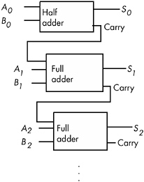
Figure 8-18: Building an n-bit adder using half and full adders
8.7.2.2 Seven-Segment LED Decoders
Another common combinatorial circuit is the seven-segment decoder . Decoder circuits are among the more important circuits in computer system design - they provide the ability to recognize (or decode ) a string of bits.
The seven-segment decoder circuit accepts an input of four bits and determines which segments to illuminate on a seven-segment LED display. Because a seven-segment display contains seven output values (one for each segment), there will be seven logic functions associated with it (segments zero through six). See Figure 8-19 for the segment assignments. Figure 8-20 shows the active segments for each of the ten decimal values.
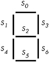
Figure 8-19: Seven-segment display
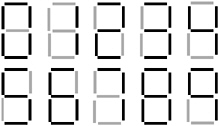
Figure 8-20: Seven-segment values for '0' through '9'
The four inputs to each of these seven Boolean functions are the four bits from a binary number in the range 0..9. Let D be the HO bit of this number and A be the LO bit. Each segment's logic function should produce a one (segment on) for all binary number inputs that have that segment illuminated in Figure 8-20. For example, S 4 (segment four) should be illuminated for numbers zero, two, six, and eight, which correspond to the binary values 0000, 0010, 0110, and 1000. For each of the binary values that illuminates a segment, you will have one minterm in the logic equation:
S 4 = D'C'B'A' + D'C'BA' + D'CBA' + DC'B'A'
S (segment zero), as a second example, is on for the numbers zero, two, three, five, six, seven, eight, and nine, which correspond to the binary values 0000, 0010, 0011, 0101, 0110, 0111, 1000, and 1001. Therefore, the logic function for S is as follows :
S = D'C'B'A' + D'C'BA' + D'C'BA + D'CB'A + D'CBA' + D'CBA + DC'B'A' + DC'B'A
8.7.2.3 Decoding Memory Addresses
A decoder is also commonly used in memory expansion. For example, suppose a system designer wishes to install four (identical) 256-MB memory modules in a system to bring the total to 1 GB of RAM. Each of these 256-MB memory modules has 28 address lines (A ..A 27 ), assuming each memory module is eight bits wide (2 28 — 8 bits is 256 MB). [1]
Unfortunately, if the system designer hooked up those four memory modules to the CPU's address bus, each of the modules would respond to the same addresses on the bus. Pandemonium would result. To correct this problem, each memory module needs to respond to a different set of addresses appearing on the address bus. By adding a chip-select line to each of the memory modules, and using a two-input, four-output decoder circuit, we can easily do this. See Figure 8-21 for the details.
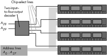
Figure 8-21: Adding four 256-MB memory modules to a system
The two-line -to-four-line decoder circuit in Figure 8-21 actually incor-porates four different logic functions: one function for each of the outputs. Assuming the inputs are A and B ( A = A 28 and B = A 29 ), then the four output functions are as follows:
Q = A'B' Q 1 = AB' Q 2 = A'B Q 3 = AB
Following standard electronic circuit notation, these equations use Q to denote an output. Also note that most circuit designers use active low logic for decoders and chip enables. This means that they enable a circuit when a low-input value (zero) is supplied and disable the circuit when a high-input value (one) is supplied. In a similar fashion, all the output lines of a decoder chip are normally high, and when the input values A and B select one particular output line, that line goes low. This means that these equations really need to be inverted for real-world examples. We have ignored this issue here and have used positive (or active high) logic.
8.7.2.4 Decoding Machine Instructions
Decoding circuits are also used to decode machine instructions. We'll cover this subject in much greater depth in Chapters 9 and 10, but a simple example is in order here.
Most modern computer systems represent machine instructions using binary values in memory. To execute an instruction, the CPU fetches the instruction's binary value from memory, decodes that value using decoder circuitry, and then does the appropriate work. To see how this is done, let's create a very simple CPU with a very simple instruction set. Figure 8-22 provides the instruction format (all the numeric codes that correspond to the various instructions) for our simple CPU.
| Warning | Do not conclude that the instruction format used in this example applies to any particular CPU's instruction set. The instruction format here is highly simplified to demonstrate instruction decoding. |
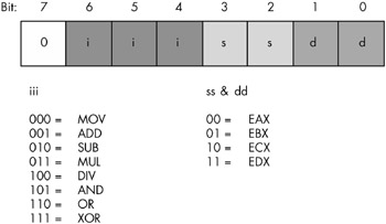
Figure 8-22: Instruction (opcode) format for a very simple CPU
To determine the 8-bit operation code (opcode) for a given instruction, the first thing you do is choose the instruction you want to encode. Let's pick mov(eax,ebx); as our simple example. To convert this instruction to its numeric equivalent, we follow these steps:
-
Look up the value for mov in the iii table in Figure 8-22. The corresponding value is 000, so we must substitute 000 for iii in the opcode byte.
-
Look up our source operand. The source operand is EAX, whose encoding in the source operand table ( ss & dd ) is 00. Therefore, we substitute 00 for ss in the instruction opcode.
-
Convert the destination operand to its numeric equivalent. The destination is in EBX, so we look up the value for this operand in the ss & dd table. Its value is 01, and we substitute 01 for dd in our opcode byte.
-
Assemble these three fields into the opcode byte (a packed data type), to obtain the bit value: %00000001.
Therefore, the numeric value $1 is the value for the mov(eax, ebx); instruction (see Figure 8-23).
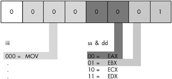
Figure 8-23: Encoding the MOV(EAX, EBX); instruction
Of course, in this example we were actually encoding the instructions. However, the real purpose of this exercise is to discover how the CPU can use a decoder circuit to decode the binary values for machine instructions and execute them at run time. A typical decoder circuit for this example appears in Figure 8-24.
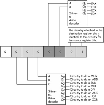
Figure 8-24: Decoding simple machine instructions
Notice how the circuit in Figure 8-24 uses three separate decoders to decode the individual fields of the opcode. This is much less complex than creating a single 7-line-to-128-line decoder to decode the entire opcode. Of course, all that the circuit in Figure 8-24 will do is tell you which instruction and what operands a given opcode specifies. To actually execute this instruction, you must supply additional circuitry to select the source and destination operands from an array of registers and act accordingly upon those operands. Such circuitry is beyond the scope of this chapter, so we'll save the juicy details for later.
8.7.3 Sequential and Clocked Logic
One major problem with combinatorial logic is that it is memoryless . In theory, all logic function outputs depend only on the current inputs. Any change in the input values immediately appears on the outputs. [2] Unfortunately, computers need the ability to remember the results of past computations . This is the domain of sequential, or clocked, logic.
8.7.3.1 The Set/Reset Flip-Flop
A memory cell is an electronic circuit that remembers an input value after the removal of that input value. The most basic memory unit is the set/reset flip-flop (S/R flip-flop). You can construct an S/R flip-flop memory cell using two NAND gates, as shown in Figure 8-25. In this diagram, you'll notice that the outputs of the two NAND gates are recirculated back to one of the inputs of the other NAND gate.
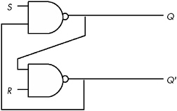
Figure 8-25: Set/reset flip flop constructed from NAND gates
The S and R inputs are normally high, or one. If you toggle the S input by temporarily setting its value to zero and then bringing it back to one, the Q output is set to one. Likewise, if you toggle the R input from one to zero and back to one, this sets the Q output to zero.
Notice that if both S and R are one, then the Q output depends upon the original value of Q itself. That is, whatever Q happens to be, the top NAND gate continues to output that same value. If Q was originally one, then the bottom NAND gate receives two inputs of one (both Q and R ), and the bottom NAND gate produces an output of zero ( Q' ). As a result, the two inputs to the top NAND gate are zero and one, and the top NAND gate produces an output of one, matching the original value for Q .
On the other hand, if the original value of Q was zero, then the inputs to the bottom NAND gate are Q = 0 and R = 1 , and the output of this bottom NAND gate is one. As a result, the inputs to the top NAND gate are S = 1 and Q' = 1 . This produces a zero output, the original value of Q .
Now suppose Q is zero, S is zero, and R is one. This sets the two inputs to the top NAND gate to one and zero, forcing the output ( Q ) to one. Return-ing S to the high state does not change the output at all, because the value of Q' is one. You will obtain this same result if Q is one, S is zero, and R is one. Again, this produces a Q output value of one, and again this value remains one even when S switches from zero to one. To overcome this and produce a Q output of one, you must toggle the S input. The same idea applies to the R input, except that toggling it forces the Q output to zero rather than to one.
There is one catch to this circuit. It does not operate properly if you set both the S and R inputs to zero simultaneously . This forces both the Q and Q' outputs to one (which is logically inconsistent). Whichever input remains zero the longest determines the final state of the flip-flop. A flip-flop operating in this mode is said to be unstable .
Table 8-9 lists all the output configurations for an S/R flip-flop based on the current inputs and the previous output values.
| Previous Q | Previous Q' | S Input | R Input | Q Output | Q' Output |
|---|---|---|---|---|---|
| x [1] | x | 0 (1 ’ ’ 1) | 1 | 1 |
|
| x | x | 1 | 0 (1 ’ ’ 1) |
| 1 |
| x | x |
|
| 1 | 1 [2] |
|
| 1 | 1 | 1 |
| 1 |
| 1 |
| 1 | 1 | 1 |
|
| [1] x = don't care , implying that the value may be zero or one and it won't affect the outputs. [2] This is an unstable configuration and will change once S or R are set to one. | |||||
8.7.3.2 The D Flip-Flop
The only problem with the S/R flip-flop is that to be able to remember either a zero or a one value, you must have two different inputs. A memory cell would be more valuable to us if we could specify the data value to remember with one input value and supply a second clock input value to latch the data input value. [3] This type of flip-flop, the D flip-flop ( D stands for data ) uses the circuit in Figure 8-26.
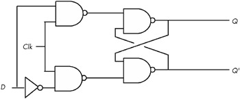
Figure 8-26: Implementing a D flip-flop with NAND gates
Assuming you fix the Q and Q' outputs to either 0/1 or 1/0, sending a clock pulse that goes from zero to one and back to zero will copy the D input to the Q output (and set Q' to the inverse of Q ). To see how this works, just note that the right half of the circuit diagram in Figure 8-26 is an S/R flip-flop. If the data input is one while the clock line is high, this places a zero on the S input of the S/R flip-flop (and a one on the R input). Conversely, if the data input is zero while the clock line is high, this places a zero on the R input (and a one on the S input) of the S/R flip-flop, thus clearing the S/R flip-flop's output. Whenever the clock input is low, both the S and R input are high, and the outputs of the S/R flip-flop do not change.
Although remembering a single bit is often important, in most computer systems you will want to remember a group of bits. You can do this by combining several D flip-flops in parallel. Concatenating flip-flops to store an n -bit value forms a register. The electronic schematic in Figure 8-27 shows how to build an 8-bit register from a set of D flip-flops.
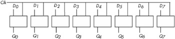
Figure 8-27: An 8-bit register implemented with eight D flip-flops
Note that the eight D flip-flops in Figure 8-27 use a common clock line. This diagram does not show the Q' outputs on the flip-flops because they are rarely required in a register.
D flip-flops are useful for building many sequential circuits beyond simple registers. For example, you can build a shift register that shifts the bits one position to the left on each clock pulse. A 4-bit shift register appears in Figure 8-28.
Figure 8-28: A 4-bit shift register built from D flip-flops
You can even build a counter that counts the number of times the clock toggles from one to zero and back to one using flip-flops. The circuit in Figure 8-29 implements a four bit counter using D flip-flops.
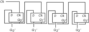
Figure 8-29: A 4-bit counter built from D flip-flops
Surprisingly, you can build an entire CPU with combinatorial circuits and only a few additional sequential circuits. For example, you can build a simple state machine known as a sequencer by combining a counter and a decoder, as shown in Figure 8-30.
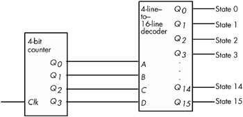
Figure 8-30: A simple 16-state sequencer
For each cycle of the clock in Figure 8-30, this sequencer activates one of its output lines. Those lines, in turn , may control other circuits. By 'firing' those other circuits on each of the 16 output lines of the decoder, we can control the order in which the circuits accomplish their tasks . This is essential in a CPU, as we often need to control the sequence of various operations. For example, it wouldn't be a good thing if the add(eax,ebx); instruction stored the result into EBX before fetching the source operand from EAX (or EBX). A simple sequencer such as this one can tell the CPU when to fetch the first operand, when to fetch the second operand, when to add them together, and when to store the result away. However, we're getting a little ahead of ourselves ; we'll discuss this in detail in the next two chapters.
[1] Actually, most memory modules are wider than eight bits, so a real 256-MB memory module will have fewer than 28 address lines, but we will ignore this technicality in this example.
[2] In practice, there is a short propagation delay between a change in the inputs and the corresponding outputs in any electronic implementation of a Boolean function.
[3] 'Latch' simply means to remember the value. That is, a D flip-flop is the basic memory element because it can remember one data bit appearing on its D input.
EAN: 2147483647
Pages: 144