Processor Specifications
| Many confusing specifications often are quoted in discussions of processors. The following sections discuss some of these specifications, including the data bus, address bus, and speed. The next section includes a table that lists the specifications of virtually all PC processors. Processors can be identified by two main parameters: how wide they are and how fast they are. The speed of a processor is a fairly simple concept. Speed is counted in megahertz (MHz) and gigahertz (GHz), which means millions and billions, respectively, of cycles per secondand faster is better! The width of a processor is a little more complicated to discuss because three main specifications in a processor are expressed in width. They are
Note that the processor data bus is also called the front side bus (FSB), processor side bus (PSB), or just CPU bus. All these terms refer to the bus that is between the CPU and the main chipset component (North Bridge or Memory Controller Hub). Intel uses the FSB or PSB terminology, whereas AMD uses only FSB. Personally I usually just like to say "CPU bus" in conversation or when speaking during my training seminars because that is the least confusing of the terms while also being completely accurate. The number of bits a processor is designated can be confusing. All modern processors have 64-bit data buses; however, that does not mean they are classified as 64-bit processors. Processors such as the Pentium 4 and Athlon XP are 32-bit processors because their internal registers are 32 bits wide, although their data I/O buses are 64 bits wide and their address buses are 36 bits wide (both wider than their predecessors, the Pentium and K6 processors). The Itanium series and the AMD Opteron and Athlon 64 are 64-bit processors because their internal registers are 64 bits wide. First, I'll present some tables describing the differences in specifications between all the PC processors; then the following sections will explain the width and other specifications in more detail. Refer to these tables as you read about the various processor specifications, and the information in the tables will become clearer. Tables 3.13.4 list the Intel processors, AMD processors, and alternative processors from other manufacturers.
Data I/O BusPerhaps the most important features of a processor are the speed and width of its external data bus. This defines the rate at which data can be moved into or out of the processor. The processor bus discussed most often is the external data busthe bundle of wires (or pins) used to send and receive data. The more signals that can be sent at the same time, the more data can be transmitted in a specified interval and, therefore, the faster (and wider) the bus. A wider data bus is like having a highway with more lanes, which enables greater throughput. Data in a computer is sent as digital information in which certain voltages or voltage transitions occurring within specific time intervals are used to represent data as 1s and 0s. The more wires you have, the more individual bits you can send in the same time interval. All modern processors from the original Pentium through the latest Pentium 4, Athlon XP, Athlon 64, and even the Itanium and Itanium 2 have a 64-bit (8-byte) wide data bus. Therefore, they can transfer 64 bits of data at a time to and from the motherboard chipset or system memory. A good way to understand this flow of information is to consider a highway and the traffic it carries. If a highway has only one lane for each direction of travel, only one car at a time can move in a certain direction. If you want to increase traffic flow, you can add another lane so that twice as many cars pass in a specified time. You can think of an 8-bit chip as being a single-lane highway because 1 byte flows through at a time. (1 byte equals 8 individual bits.) The 16-bit chip, with 2 bytes flowing at a time, resembles a two-lane highway. You might have four lanes in each direction to move a large number of automobiles; this structure corresponds to a 32-bit data bus, which has the capability to move 4 bytes of information at a time. Taking this further, a 64-bit data bus is like having an 8-lane highway moving data in and out of the chip. Another ramification of the data bus in a chip is that the width of the data bus also defines the size of a bank of memory. So, a processor with a 32-bit data bus (such as the 486) reads and writes memory 32 bits at a time, whereas processors with a 64-bit data bus (most current processors) read and write memory 64 bits at a time. In 486 class systems, because standard 72-pin single inline memory modules (SIMMs) are only 32 bits wide, they must be installed one at a time in most 486 class systems. When used in 64-bit Pentium class systems, they must be installed two at a time. The current module standard, dual inline memory modules (DIMMs), are 64 bits wide. So, they are normally installed one at a time, unless the system is designed or configured for dual-channel memory. Dual-channel memory reads and writes two banks simultaneously, as a way to improve system performance, which means two DIMMs must be installed at a time. To improve memory performance, most future chipsets will support and eventually require that DIMM memory modules be installed in identical pairs. The Rambus inline memory modules (RIMMs) used in some older Pentium III and 4 systems are somewhat of an anomaly because they play by a different set of rules. They are typically only 16 or 32 bits wide. Depending on the module type and chipset, they are either used individually or in pairs.
Address BusThe address bus is the set of wires that carries the addressing information used to describe the memory location to which the data is being sent or from which the data is being retrieved. As with the data bus, each wire in an address bus carries a single bit of information. This single bit is a single digit in the address. The more wires (digits) used in calculating these addresses, the greater the total number of address locations. The size (or width) of the address bus indicates the maximum amount of RAM a chip can address. The highway analogy in the "Data I/O Bus" section can be used to show how the address bus fits in. If the data bus is the highway and the size of the data bus is equivalent to the number of lanes, the address bus relates to the house number or street address. The size of the address bus is equivalent to the number of digits in the house address number. For example, if you live on a street in which the address is limited to a two-digit (base 10) number, no more than 100 distinct addresses (0099) can exist for that street (102). Add another digit, and the number of available addresses increases to 1,000 (000999), or 103. Computers use the binary (base 2) numbering system, so a two-digit number provides only four unique addresses (00, 01, 10, and 11), calculated as 22. A three-digit number provides only eight addresses (000111), which is 23. For example, the 8086 and 8088 processors use a 20-bit address bus that calculates as a maximum of 220 or 1,048,576 bytes (1MB) of address locations. Table 3.5 describes the memory-addressing capabilities of processors.
The data bus and address bus are independent, and chip designers can use whatever size they want for each. Usually, however, chips with larger data buses have larger address buses. The sizes of the buses can provide important information about a chip's relative power, measured in two important ways. The size of the data bus is an indication of the chip's information-moving capability, and the size of the address bus tells you how much memory the chip can handle. Internal Registers (Internal Data Bus)The size of the internal registers indicates how much information the processor can operate on at one time and how it moves data around internally within the chip. This is sometimes also referred to as the internal data bus. A register is a holding cell within the processor; for example, the processor can add numbers in two different registers, storing the result in a third register. The register size determines the size of data on which the processor can operate. The register size also describes the type of software or commands and instructions a chip can run. That is, processors with 32-bit internal registers can run 32-bit instructions that are processing 32-bit chunks of data, but processors with 16-bit registers can't. Most advanced processors todaychips from the 386 to the Pentium 4use 32-bit internal registers and can therefore run the same 32-bit operating systems and software. The Itanium and Athlon 64 processors have 64-bit internal registers, which require new operating systems and software to fully be utilized. Some very old processors have an internal data bus (made up of data paths and storage units called registers) that is larger than the external data bus. The 8088 and 386SX are examples of this structure. Each chip has an internal data bus twice the width of the external bus. These designs, which sometimes are called hybrid designs, usually are low-cost versions of a "pure" chip. The 386SX, for example, can pass data around internally with a full 32-bit register size; for communications with the outside world, however, the chip is restricted to a 16-bit-wide data path. This design enabled a systems designer to build a lower-cost motherboard with a 16-bit bus design and still maintain software and instruction set compatibility with the full 32-bit 386. However, both the 8088 and the 386SX had lower performance than the 8086 and 386DX processors at the same speeds. Internal registers often are larger than the data bus, which means the chip requires two cycles to fill a register before the register can be operated on. For example, both the 386SX and 386DX have internal 32-bit registers, but the 386SX must "inhale" twice (figuratively) to fill them, whereas the 386DX can do the job in one "breath." The same thing would happen when the data is passed from the registers back out to the system bus. The Pentium is an example of this type of design. All Pentiums have a 64-bit data bus and 32-bit registersa structure that might seem to be a problem until you understand that the Pentium has two internal 32-bit pipelines for processing information. In many ways, the Pentium is like two 32-bit chips in one. The 64-bit data bus provides for very efficient filling of these multiple registers. Multiple pipelines are called superscalar architecture, which was introduced with the Pentium processor.
More advanced sixth- and seventh-generation processors from Intel and AMD have as many as six internal pipelines for executing instructions. Although some of these internal pipes are dedicated to special functions, these processors can execute multiple operations in one clock cycle. Processor ModesAll Intel and Intel-compatible 32-bit processors (from the 386 on up) can run in several modes. Processor modes refer to the various operating environments and affect the instructions and capabilities of the chip. The processor mode controls how the processor sees and manages the system memory and the tasks that use it. The three main modes of operation with several submodes are as follows:
Table 3.6 summarizes the processor modes.
Real ModeReal mode is sometimes called 8086 mode because it is based on the 8086 and 8088 processors. The original IBM PC included an 8088 processor that could execute 16-bit instructions using 16-bit internal registers and could address only 1MB of memory using 20 address lines. All original PC software was created to work with this chip and was designed around the 16-bit instruction set and 1MB memory model. For example, DOS and all DOS software, Windows 1.x through 3.x, and all Windows 1.x through 3.x applications are written using 16-bit instructions. These 16-bit operating systems and applications are designed to run on an original 8088 processor.
Later processors such as the 286 could also run the same 16-bit instructions as the original 8088, but much faster. In other words, the 286 was fully compatible with the original 8088 and could run all 16-bit software just the same as an 8088, but, of course, that software would run faster. The 16-bit instruction mode of the 8088 and 286 processors has become known as real mode. All software running in real mode must use only 16-bit instructions and live within the 20-bit (1MB) memory architecture it supports. Software of this type is usually single-taskingonly one program can run at a time. No built-in protection exists to keep one program from overwriting another program or even the operating system in memory, so if more than one program is running, one of them could bring the entire system to a crashing halt. IA-32 Mode (32-Bit)Then came the 386, which was the PC industry's first 32-bit processor. This chip could run an entirely new 32-bit instruction set. To take full advantage of the 32-bit instruction set, a 32-bit operating system and a 32-bit application were required. This new 32-bit mode was referred to as protected mode, which alludes to the fact that software programs running in that mode are protected from overwriting one another in memory. Such protection helps make the system much more crash-proof because an errant program can't very easily damage other programs or the operating system. In addition, a crashed program can be terminated while the rest of the system continues to run unaffected. Knowing that new operating systems and applicationswhich take advantage of the 32-bit protected modewould take some time to develop, Intel wisely built a backward compatible real mode into the 386. That enabled it to run unmodified 16-bit operating systems and applications. It ran them quite wellmuch more quickly than any previous chip. For most people, that was enough. They did not necessarily want any new 32-bit software; they just wanted their existing 16-bit software to run more quickly. Unfortunately, that meant the chip was never running in the 32-bit protected mode, and all the features of that capability were being ignored. When a high-powered processor such as a Pentium 4 is running DOS (real mode), it acts like a "Turbo 8088." Turbo 8088 means the processor has the advantage of speed in running any 16-bit programs; it otherwise can use only the 16-bit instructions and access memory within the same 1MB memory map of the original 8088. Therefore, if you have a 256MB Pentium 4 or Athlon system running Windows 3.x or DOS, you are effectively using only the first megabyte of memory, leaving the other 255MB largely unused! New operating systems and applications that ran in the 32-bit protected mode of the modern processors were needed. Being stubborn, we resisted all the initial attempts at getting switched over to a 32-bit environment. It seems that as a user community, we are very resistant to change and would be content with our older software running faster rather than adopting new software with new features. I'll be the first one to admit that I was one of those stubborn users myself! Because of this resistance, true 32-bit operating systems such as Unix or variants (such as Linux), OS/2, and even Windows NT/2000 or XP have taken a long time in getting a mainstream share in the PC marketplace. Windows XP is the first full 32-bit OS that has become a true mainstream product, and that is primarily because Microsoft has coerced us in that direction with Windows 95, 98, and Me (which are mixed 16-/32-bit systems). Windows 3.x was the last full 16-bit operating system. In fact, it was not really considered a complete operating system because it ran on top of DOS. The Itanium processor family, the AMD Opteron, and the Intel EM64T-compatible Xeon processors add 64-bit native capability to the table for servers, whereas the AMD Athlon 64 family, the Intel EM64T-compatible Pentium 4, and all Intel Pentium D processors provide this capability for desktop computers. Both processors run all the existing 32-bit software, but to fully take advantage of the processor, a 64-bit OS, drivers, and applications are required. Microsoft has released 64-bit versions of Windows XP, and several companies have released 64-bit applications for networking and workstation use. Note The Intel Itanium family uses the Intel-designed EPIC processor architecture. However, the AMD Athlon 64, the Opteron, and some Semprons use an AMD-developed extension of the x86 architecture Intel originally developed for 386 and higher processors. This architecture is sometimes referred to as IA32e, but AMD refers to this design as AMD64 and Intel uses the term EM64T to refer to its virtually identical 64-bit technology for the Pentium D, Pentium Extreme Edition, and 64-bit versions of the Pentium 4 desktop and Xeon workstation/server processors. Because EPIC and AMD64/EM64T architectures are different, 64-bit software written for one architecture will not work on the other without being recompiled by the software vendor. This means that software written specifically for the Intel EPIC 64-bit architecture will not run on AMD64/EM64T 64-bit processors, and vice versa. IA-32 Virtual Real ModeThe key to the backward compatibility of the Windows 32-bit environment is the third mode in the processor: virtual real mode. Virtual real is essentially a virtual real mode 16-bit environment that runs inside 32-bit protected mode. When you run a DOS prompt window inside Windows, you have created a virtual real mode session. Because protected mode enables true multitasking, you can actually have several real mode sessions running, each with its own software running on a virtual PC. These can all run simultaneously, even while other 32-bit applications are running. Note that any program running in a virtual real mode window can access up to only 1MB of memory, which that program will believe is the first and only megabyte of memory in the system. In other words, if you run a DOS application in a virtual real window, it will have a 640KB limitation on memory usage. That is because there is only 1MB of total RAM in a 16-bit environment and the upper 384KB is reserved for system use. The virtual real window fully emulates an 8088 environment, so that aside from speed, the software runs as if it were on an original real mode-only PC. Each virtual machine gets its own 1MB address space, an image of the real hardware BIOS routines, and emulation of all other registers and features found in real mode. Virtual real mode is used when you use a DOS window to run a DOS or Windows 3.x 16-bit program. When you start a DOS application, Windows creates a virtual DOS machine under which it can run. One interesting thing to note is that all Intel and Intel-compatible (such as AMD and Cyrix) processors power up in real mode. If you load a 32-bit operating system, it automatically switches the processor into 32-bit mode and takes control from there. It's also important to note that some 16-bit (DOS and Windows 3.x) applications misbehave in a 32-bit environment, which means they do things that even virtual real mode does not support. Diagnostics software is a perfect example of this. Such software does not run properly in a real-mode (virtual real) window under Windows. In that case, you can still run your Pentium 4 in the original no-frills real mode by either booting to a DOS floppy or, in the case of Windows 9x (excluding Me), interrupting the boot process and commanding the system to boot plain DOS. This is accomplished on Windows 9x systems by pressing the F8 key when you see the prompt Starting Windows... on the screen or immediately after the beep when the power on self test (POST) is completed. In the latter case, it helps to press the F8 key multiple times because getting the timing just right is difficult and Windows 9x looks for the key only during a short two-second time window. If successful, you will then see the Startup menu. You can select one of the command-prompt choices that tell the system to boot plain 16-bit real mode DOS. The choice of Safe Mode Command Prompt is best if you are going to run true hardware diagnostics, which do not normally run in protected mode and should be run with a minimum of drivers and other software loaded. Even though Windows Me is based on Windows 98, Microsoft removed the DOS Startup menu option in an attempt to further wean us from any 16-bit operation. Windows NT, 2000, and XP also lack the capability to start up DOS in this manner. For these operating systems, you need a startup disk (CD or floppy), which you can use to boot the system in real mode. Generally, you would do this to perform certain maintenance procedures, such as running hardware diagnostics or doing direct disk sector editing. Although real mode is used by 16-bit DOS and "standard" DOS applications, special programs are available that "extend" DOS and allow access to extended memory (over 1MB). These are sometimes called DOS extenders and usually are included as part of any DOS or Windows 3.x software that uses them. The protocol that describes how to make DOS work in protected mode is called DOS protected mode interface (DPMI). DPMI was used by Windows 3.x to access extended memory for use with Windows 3.x applications. It allowed these programs to use more memory even though they were still 16-bit programs. DOS extenders are especially popular in DOS games because they enable them to access much more of the system memory than the standard 1MB most real mode programs can address. These DOS extenders work by switching the processor in and out of real mode. In the case of those that run under Windows, they use the DPMI interface built into Windows, enabling them to share a portion of the system's extended memory. Another exception in real mode is that the first 64KB of extended memory is actually accessible to the PC in real mode, despite the fact that it's not supposed to be possible. This is the result of a bug in the original IBM AT with respect to the 21st memory address line, known as A20 (A0 is the first address line). By manipulating the A20 line, real-mode software can gain access to the first 64KB of extended memorythe first 64KB of memory past the first megabyte. This area of memory is called the high memory area (HMA). IA-32e 64-Bit Extension Mode (AMD64, x86-64, EM64T)64-bit extension mode is an enhancement to the IA-32 architecture originally designed by AMD and later adopted by Intel. Processors with 64-bit extension technology can run in real (8086) mode, IA-32 mode, or IA-32e mode. IA-32 mode enables the processor to run in protected mode and virtual real mode. IA-32e mode allows the processor to run in 64-bit mode and compatibility mode, which means you can run both 64-bit and 32-bit applications simultaneously. IA-32e mode includes two submodes:
IA-32e 64-bit mode is enabled by loading a 64-bit operating system and is used by 64-bit applications. In the 64-bit submode, the following new features are available:
IE-32e compatibility mode enables 32-bit and 16-bit applications to run under a 64-bit operating system. Unfortunately, legacy 16-bit programs that run in virtual real mode (that is, DOS programs) are not supported and will not run, which is likely to be the biggest problem for many users. Similar to 64-bit mode, compatibility mode is enabled by the operating system on an individual code basis, which means 64-bit applications running in 64-bit mode can operate simultaneously with 32-bit applications running in compatibility mode. What we need to make all this work is a 64-bit operating system and, more importantly, 64-bit drivers for all our hardware to work under that OS. A 64-bit OS already exists in two versions:
Of those, the first is for IA-64 processors, such as Itanium and Itanium 2, and has been available in a released production version since 2001. The latter is for IA-32 processors with 64-bit extensions, such as the Athlon 64, Opteron, some Semprons, the Pentium D, the Pentium Extreme Edition, and some Xeon and Pentium 4 processors supporting 64-bit extensions, and is now available on shipping systems, as an upgrade from Windows XP Professional, or as a 360-day trial version. Note that Microsoft uses the term x64 to refer to processors that support either AMD64 or EM64T because AMD and Intel's extensions to the standard IA32 architecture are practically identical and can be supported with a single version of Windows. Note Early versions of EM64T-equipped processors from Intel lacked support for the LAHF and SAHF instructions used in the AMD64 instruction set. However, Pentium 4 and Xeon DP processors using core steppings G1 and higher completely support these instructions; a BIOS update is also needed. The differences between Windows XP 32-bit and 64-bit versions are shown in Table 3.7.
The major difference between 32-bit and 64-bit Windows XP is memory support, specifically breaking the 4GB barrier found in 32-bit Windows systems. Windows XP 32-bit supports up to 4GB of physical or virtual memory, with up to 2GB of dedicated memory per process. Windows XP 64-bit Edition supports up to 128GB of physical memory and up to 16TB of virtual memory. Support for more memory means applications can preload more data into either physical or virtual memory, which the processor can access much more quickly. If you need more than 4GB of RAM, 64-bit systems and 64-bit Windows are required. Windows XP 64-bit runs 32-bit Windows applications with no problems, but it does not run DOS applications or other programs that run in virtual real mode. Also, drivers are another big problem. 32-bit processes cannot load 64-bit dynamic link libraries (DLLs), and 64-bit processes cannot load 32-bit DLLs. This essentially means that, for all the devices you have connected to your system, you need both 32-bit and 64-bit drivers for them to work. Acquiring 64-bit drivers for older devices or devices that are no longer supported can be difficult or impossible. Even for new devices, it can be a couple of years before manufacturers provide 64-bit drivers as a standard feature. Before installing a 64-bit version of Windows, be sure to check with the vendors of your internal and add-on hardware for 64-bit drivers. Keep in mind that drivers made for Itanium do not work with x64-compatible processors. You should keep all the memory size, software, and driver issues in mind when considering the transition from 32-bit to 64-bit technology. The transition from 32-bit hardware to mainstream 32-bit computing took 16 years. As I've already stated, it might not take 16 years for 64-bit computing to become mainstream, but it will most likely take at least a few years. Processor Speed RatingsA common misunderstanding about processors is their different speed ratings. This section covers processor speed in general and then provides more specific information about Intel, AMD, and VIA/Cyrix processors. A computer system's clock speed is measured as a frequency, usually expressed as a number of cycles per second. A crystal oscillator controls clock speeds using a sliver of quartz sometimes contained in what looks like a small tin container. Newer systems include the oscillator circuitry in the motherboard chipset, so it might not be a visible separate component on newer boards. As voltage is applied to the quartz, it begins to vibrate (oscillate) at a harmonic rate dictated by the shape and size of the crystal (sliver). The oscillations emanate from the crystal in the form of a current that alternates at the harmonic rate of the crystal. This alternating current is the clock signal that forms the time base on which the computer operates. A typical computer system runs millions or billions of these cycles per second, so speed is measured in megahertz or gigahertz. (One hertz is equal to one cycle per second.) An alternating current signal is like a sine wave, with the time between the peaks of each wave defining the frequency (see Figure 3.1). Figure 3.1. Alternating current signal showing clock cycle timing. Note The hertz was named for the German physicist Heinrich Rudolf Hertz. In 1885, Hertz confirmed the electromagnetic theory, which states that light is a form of electromagnetic radiation and is propagated as waves. A single cycle is the smallest element of time for the processor. Every action requires at least one cycle and usually multiple cycles. To transfer data to and from memory, for example, a modern processor such as the Pentium 4 needs a minimum of three cycles to set up the first memory transfer and then only a single cycle per transfer for the next three to six consecutive transfers. The extra cycles on the first transfer typically are called wait states. A wait state is a clock tick in which nothing happens. This ensures that the processor isn't getting ahead of the rest of the computer.
The time required to execute instructions also varies:
Different instruction execution times (in cycles) make comparing systems based purely on clock speed or number of cycles per second difficult. How can two processors that run at the same clock rate perform differently with one running "faster" than the other? The answer is simple: efficiency. The main reason the 486 was considered fast relative to a 386 is that it executes twice as many instructions in the same number of cycles. The same thing is true for a Pentium; it executes about twice as many instructions in a given number of cycles as a 486. Therefore, given the same clock speed, a Pentium is twice as fast as a 486, and consequently a 133MHz 486 class processor (such as the AMD 5x86-133) is not even as fast as a 75MHz Pentium! That is because Pentium megahertz are "worth" about double what 486 megahertz are worth in terms of instructions completed per cycle. The Pentium II and III are about 50% faster than an equivalent Pentium at a given clock speed because they can execute about that many more instructions in the same number of cycles. Unfortunately, after the Pentium III, it becomes much more difficult to compare processors on clock speed alone. This is because the different internal architectures make some processors more efficient than others, but these same efficiency differences result in circuitry that is capable of running at different maximum speeds. The less efficient the circuit, the higher the clock speed it can attain, and vice versa. Comparing relative processor performance, you can see that a 1GHz Pentium III is about equal to a (theoretical) 1.5GHz Pentium, which is about equal to a 3GHz 486, which is about equal to a 6GHz 386 or 286, which is about equal to a 12GHz 8088. The original PC's 8088 ran at only 4.77MHz; today, we have systems that are comparatively at least 2,500 times faster! As you can see, you must be careful in comparing systems based on pure MHz alone because many other factors affect system performance. Evaluating CPU performance can be tricky. CPUs with different internal architectures do things differently and can be relatively faster at certain things and slower at others. To fairly compare various CPUs at different clock speeds, Intel has devised a specific series of benchmarks called the iCOMP (Intel Comparative Microprocessor Performance) index that can be run against processors to produce a relative gauge of performance. The iCOMP index benchmark has been updated twice and released in original iCOMP, iCOMP 2.0, and now iCOMP 3.0 versions. Table 3.8 shows the relative power, or iCOMP 2.0 index, for several processors.
Note Note that this reflects the most recent iCOMP index. Intel uses other benchmarks for the Pentium 4 and subsequent processors. The iCOMP 2.0 index is derived from several independent benchmarks and is a stable indication of relative processor performance. The benchmarks balance integer with floating-point and multimedia performance. When Intel developed the Pentium III, it discontinued the iCOMP 2.0 index and released the iCOMP 3.0 index. iCOMP 3.0 is an updated benchmark that incorporates an increasing use of 3D, multimedia, and Internet technology and software, as well as the increasing use of rich data streams and computer-intensive applications, including 3D, multimedia, and Internet technology. iCOMP 3.0 combines six benchmarks: WinTune 98 Advanced CPU Integer test, CPUmark 99, 3D WinBench 99-3D Lighting and Transformation Test, MultimediaMark 99, Jmark 2.0 Processor Test, and WinBench 99-FPU WinMark. These newer benchmarks take advantage of the SSE (Streaming SIMD Extensions), additional graphics and sound instructions built into the PIII. Without taking advantage of these new instructions, the PIII would benchmark at about the same speed as a PII at the same clock rate. Table 3.9 shows the iCOMP Index 3.0 ratings for Pentium II and III processors.
Intel and AMD currently rate their latest processors using the commercially available BAPCo SYSmark 2002 and 2004 benchmark suites. The ratings for the various processors under the 2002 and 2004 benchmark suites are shown in Tables 3.10 and 3.11.
SYSmark 2002 and 2004 are commercially available application-based benchmarks that reflect the normal usage of business users employing modern Internet content creation and Microsoft Office applications. However, it is important to note that the scores listed here are produced by complete systems and are affected by things such as the specific version of the processor, the motherboard and chipset used, the amount and type of memory installed, the speed of the hard disk, and other factors. For complete disclosure of the other factors resulting in the given scores, see the BAPCo website. SYSmark 2002 incorporates the following applications, which it uses for testing:
SYSmark 2004 incorporates the following applications, which it uses for testing:
The latest version of SYSmarkSYSmark 2004 SEwas introduced in June 2005 and now supports the Windows XP Professional x64 Edition. SYSmark 2004 SE uses the same applications used by SYSmark 2004, but it incorporates changes to its operation that are designed to more closely mirror how a typical user works with the application mix featured in each module. SYSmark runs various scripts to do actual work using these applications and is used by many companies for testing and comparing PC systems and components. It is a much more modern and real-world benchmark than the iCOMP benchmark Intel previously used, and because it is available to anybody, the results can be independently verified. SYSmark 2002, 2004, and 2004SE can be purchased from BAPCo at www.bapco.com or from FutureMark at www.futuremark.com. Processor Speeds and Markings Versus Motherboard SpeedAnother confusing factor when comparing processor performance is that virtually all modern processors since the 486DX2 run at some multiple of the motherboard speed. For example, a Pentium 4 2.53GHz chip runs at a multiple of 19/4 (4.75x) times the motherboard speed of 533MHz, whereas an AMD Athlon XP 2800+ using the latest Barton core (2.083GHz) runs at 75/12 (6.25x) times the motherboard speed of 333MHz. Up until early 1998, most motherboards ran at 66MHz or less. Starting in April 1998, Intel released both processors and motherboard chipsets designed to run at 100MHz. By late 1999, chipsets and motherboards running at 133MHz became available to support the newer Pentium III processors. At that time, AMD Athlon motherboards and chipsets were introduced running a 100MHz clock but using a double transfer technique for an effective 200MHz data rate between the Athlon processor and the main chipset North Bridge chip. In 2000 and 2001, processor bus speeds advanced further to 266MHz for the AMD Athlon and Intel Itanium and 400MHz to 533MHz for the Pentium 4. In 2002, the AMD Athlon XP processors began to support a processor bus speed of 333MHz. In 2003, Intel introduced the first Pentium 4 processors that supported a processor bus speed of 800MHz; later that year, Intel introduced the Pentium 4 Extreme Edition, which supports a processor bus speed of 1066MHz. Typically, the speed of the CPU bus is selected to match whatever memory types Intel and AMD want to support. Most of the modern CPU bus speeds are based on the speeds of the CPU as well as the available SDRAM, DDR SDRAM, and RDRAM memory. Note that the processor bus speed of Pentium 4, Pentium D, and Pentium Extreme Edition processors is not directly equivalent to a particular memory speed. Note See Chapter 4, "Motherboards and Buses," for more information on chipsets and bus speeds. You can set the motherboard speed and multiplier setting via jumpers or another configuration mechanism (such as BIOS setup) on the motherboard. Modern systems use a variable-frequency synthesizer circuit usually found in the main motherboard chipset to control the motherboard and CPU speed. Most Pentium motherboards have three or four speed settings. The processors used today are available in a variety of versions that run at different frequencies based on a given motherboard speed. For example, most of the Pentium chips run at a speed that is some multiple of the true motherboard speed. For example, Pentium-class processors and motherboards run at the speeds shown in Table 3.12.
Note For information on specific AMD, Cyrix, or VIA processors, see their respective sections later in this chapter. If all other variables are equalincluding the type of processor, the number of wait states (empty cycles) added to different types of memory accesses, and the width of the data busyou can compare two systems by their respective clock rates. However, the construction and design of the memory controller (contained in the motherboard chipset) as well as the type and amount of memory installed can have an enormous effect on a system's final execution speed. In building a processor, a manufacturer tests it at various speeds, temperatures, and pressures. After the processor is tested, it receives a stamp indicating the maximum safe speed at which the unit will operate under the wide variation of temperatures and pressures encountered in normal operation. These ratings are clearly marked on the processor package. Cyrix Processor SpeedsCyrix/IBM/VIA 6x86 processorswhich were designed to compete with the Intel Pentium, early Pentium II, and AMD K5 and K6 series of processorsused a PR (performance rating) scale that was not equal to the true clock speed in megahertz. For example, the Cyrix 6x86MX/MII-PR366 actually runs at only 250MHz (2.5x100MHz). This is a little misleadingyou must set up the motherboard as if a 250MHz processor were being installed, instead of the 366MHz you might suspect. Unfortunately, this led people to believe these systems were faster than they really were. Table 3.13 shows the relationship between the Cyrix 6x86, 6x86MX, and M-II P-Ratings versus the actual chip speeds in MHz.
Note that a given P-Rating can mean several different actual CPU speedsfor example, a Cyrix 6x86MX-PR200 might actually be running at 150MHz, 165MHz, 166MHz, or 180MHz, but not at 200MHz. This P-Rating was supposed to indicate speed in relation to an Intel Pentium processor, but the processor being compared to in this case is the original non-MMX, small L1 cache version running on an older motherboard platform with an older chipset and slower technology memory. The P-Rating did not compare well against the Celeron, Pentium II, or Pentium III processors. In other words, the MII-PR366 really ran at only 250MHz and compared well against Intel processors running at closer to that speed, making the ratings somewhat misleading. AMD Processor SpeedsAMD's Athlon XP processors were excellent performers and included several notable features, but they also brought with them a resurrection of the infamous Cyrix/AMD performance rating. This is a simulated MHz number that does not indicate the actual speed of the chip but instead indicates an estimate of the relative MHz of a first-generation Intel Pentium 4 that would be approximately equal in performance. If this sounds confusing, that's because it is! As time marched on and CPU architecture evolved, this method of rating chips had to be revised and eventually abandoned. Although AMD uses model numbers to identify the newer Sempron and Athlon 64 product families, the model numbers for these chips are not specifically intended to compare the processors to Intel processors. As is increasingly the case with both Intel and AMD processors, to gauge processor performance, there's no substitute for knowing the particular features (CPU speed, motherboard speed, L2 cache size, and so on) of a given processor. Table 3.14 shows the P-Rating (model number) and actual speeds of the AMD K5, K6, Athlon, Athlon XP, Duron, and Sempron (Socket A) processors.
The marketing problem that led to the need for performance ratings and model numbers for processors is real: How do you market a chip that performs faster than its predecessors or its rivals when both are running at the same clock speed or lower? For example, an AMD Athlon XP with an actual clock speed of 2GHz is significantly faster than a 2GHz Pentium 4 (Northwood) and in fact performs about equal to a 2.4GHz Pentium 4 (hence, AMD called its model the Athlon XP 2400+). This apparent disparity in performance is because the P4 uses a different architecture that utilizes a deeper instruction pipeline with more stages. The original version of the Pentium 4 had a 20-stage pipeline, which compared to a 10-stage pipeline in the Athlon and a 10-stage pipeline in the Pentium III/Celeron (see Table 3.15).
A deeper pipeline effectively breaks instructions down into smaller microsteps, which allows overall higher clock rates to be achieved using the same silicon technology. However, it also means that overall fewer instructions can be executed in a single cycle as compared to processors with shorter pipelines. This is because, if a branch prediction or speculative execution step fails (which happens fairly frequently inside the processor as it attempts to line up instructions in advance), the entire pipeline has to be flushed and refilled. Thus, if you compared an Athlon to a Pentium III to a Pentium 4 all running at the same clock speed, the Athlon and Pentium III would both beat the Pentium 4 running typical benchmarks because they would execute more instructions in the same number of cycles. Although this would sound bad for the Pentium 4, it really isn't. Intel's reasoning was sound: Even though the deeper pipeline might be 30% less efficient overall, it more than makes up for this by allowing at least 50% greater clock speeds than the Athlon XP or Pentium III could muster. The deeper 20- or 31-stage pipeline in the P4 architecture enables significantly higher clock speeds to be achieved using the same silicon die process as other chips. As an example, the Athlon XP and Pentium 4 were originally made using the same 0.18-micron process (which describes the line width of components etched on the chips). The P4's 20-stage pipeline enabled the 0.18-micron die process to result in chips running up to 2.0GHz, whereas the same process achieves only 1.73GHz in the 10-stage Athlon XP and only 1.13GHz in the 10-stage Pentium III/Celeron. Using the newer 0.13-micron process, the Pentium 4 runs up to 3.4GHz and the Athlon XP tops out at 2.2GHz (3200+ model) in the same introduction timeframe. The latest Pentium 4 models (and the dual-core Pentium D and Pentium Extreme Edition) use the 0.09-micron process to reach clock speeds up to 3.8GHz. Even though the Pentium 4 executes fewer instructions in each cycle, the overall higher cycling speeds make up for the loss of efficiency. So, in the end, for the initial crop of Athlon XP and Pentium 4 processors, higher clock speed versus more efficient processing effectively cancelled each other out. Note If you want to determine the designed clock speed for any type of AMD processor (the actual clock speed could vary according to motherboard overclocking, underclocking, or power management clock speed adjustments), go to AMD's website and download the Data Sheet for the processor model you are interested in. You will find a table in each data sheet that lists the actual MHz (divide by 1,000 for the GHz) for each model. One thing is clear in all of this confusion: Raw MHz (or GHz) is not always a good way to compare chips, and generating pseudo-MHz numbers can only make things more confusing for the uninitiated. Even Intel moved away from using clock speed as its primary marketing designation. It still notes the speeds of its chips, but the processors are labeled and marketed primarily by model number. This is necessary because the relative difference between each model number is based not just on the CPU's speed, but also on architectural and other differences that affect overall performance.
OverclockingAs is discussed in detail in Chapter 21, "PC Mods: Overclocking and Cooling," in some systems, the processor speed can be set higher than the rating on the chip; this is called overclocking the chip. In many cases, you can get away with a certain amount of overclocking because Intel, AMD, and others often build safety margins into their ratings. So, a chip rated for, say, 800MHz might in fact run at 900MHz or more but instead be down-rated to allow for a greater margin of reliability. By overclocking, you are using this margin and running the chip closer to its true maximum speed. I don't normally recommend overclocking for a novice, but if you are comfortable playing with your system settings, and you can afford and are capable of dealing with any potential consequences, overclocking might enable you to get 10%20% or more performance from your system. Overclocking PitfallsIf you are intent on overclocking, there are several issues to consider. One is that most Intel processors since the Pentium II are multiplier-locked before they are shipped out. Therefore, the chip ignores any changes to the multiplier setting on the motherboard. Actually, both Intel and AMD lock the multipliers on most of their newer processors, but the AMD processors use solder bridges on top of the chip that can be manipulated if you are careful and somewhat mechanically inclined. Although originally done to prevent re-markers from fraudulently relabeling processors (creating "counterfeit" chips), this has impacted the computing performance enthusiast, leaving tweaking the motherboard bus speed as the only easy way (or in some cases, the only way possible) to achieve a clock speed higher than standard. You can run into problems increasing motherboard bus speed, as well. Most older Intel motherboards, for example, simply don't support clock speeds other than the standard 66MHz, 100MHz, 133MHz, 400MHz, 533MHz or 800MHz settings. Newer Intel boards have a "burn-in" feature that allows you to increase the default processor bus speed (and also the speed of the processor core) by up to 4%. That is relatively mild, but achievable with most chips. Most other brands of motherboards allow changing the bus speeds by even greater amounts, as well as in small increments, sometimes as small as 1MHz changes. Small incremental changes in clock multiplier speeds, rather than large jumps, are the best way to coax a bit more performance out of a particular processor. This is because a given chip is generally overclockable by a certain percentage. The smaller the steps you can take when increasing speed, the more likely that you'll be able to come close to the actual maximum speed of the chip without going over that amount and causing system instability. For example, the Asus P5LD2 motherboard for Socket 775 Pentium 4 processors supports the standard motherboard bus speeds of 533MHz, 800MHz, and 1066MHz. However, it also permits 1MHz adjustments of the front-side bus (which is multiplied by 4 to obtain the motherboard bus) to enable you to fine-tune your processor speed. Assume you have a 2.8GHz processor with an 800MHz motherboard (FSB) bus. The CPU frequency is 200MHz and is multiplied by 4 to obtain the motherboard bus (FSB) speed: 800MHz x 3.5 = 2800MHz, or 2.8GHz. Here are the actual speeds you could achieve by adjusting the CPU frequency from 200MHz (the standard setting for Intel CPUs with an 800MHz motherboard bus or FSB) to 220MHz:
Typically, a 10%20% increase is successful, especially if your system offers excellent cooling and you can also adjust CPU voltage and other settings. So with this motherboard, you are likely to get your processor running 200MHz or faster than it was originally designed for. An issue when it comes to increasing CPU bus speeds is that the other buses in the system will typically be similarly affected. Thus, if you increase the CPU bus speed by 10%, you might also be increasing the PCI or AGP bus by the same amount, and your video, network, or other cards might not be able to keep up. This is something that varies from board to board, so you have to consider each example as a potentially unique case. If possible, configure the AGP and PCI buses to run at their normal speeds through the appropriate BIOS settings. Overclocking Socket A ProcessorsThe AMD Athlon and Duron processors in the FC-PGA (flip-chip pin grid array) format, which plugs into Socket A, have special solder bridges on the top face of the chip that can be modified to change or remove the lock from the internal multiplier on the chip. This can increase the speed of the chip without changing the motherboard bus speed, thus affecting other buses or cards. The selected multiplier is set or locked by very small solder connections between solder dots (contacts) on the surface of the chip. You can completely unlock the chip by bridging or disconnecting the appropriate dots. Unfortunately, it is somewhat difficult to add or remove these bridges; you usually have to mask off the particular bridge you want to create and, rather than dripping solder onto it, literally paint the bridge with silver or copper paint. For example, you can use the special copper paint sold in small vials at any auto parts store for repairing the window defogger grids. The real problem is that the contacts are very small, and if you bridge to adjacent rather than opposite contacts, you can render the chip nonfunctional. An Xacto knife or razor blade can be used to remove the bridges if desired. If you are not careful, you can easily damage a processor worth several hundred dollars. If you are leery of making such changes, you should try bus overclocking instead because this is done in the BIOS Setup and can easily be changed or undone without any mechanical changes to the chip. CPU Voltage SettingsAnother trick used by overclockers is playing with the voltage settings for the CPU. All modern CPU sockets and slots, including Slot 1, Slot A, Socket 8, Socket 370, Socket 423, Socket 462 (Socket A), Socket 478, Socket 754, Socket 775, Socket 939, and Socket 940, have automatic voltage detection. With this detection, the system detects and sets the correct voltage by reading certain pins on the processor. Some motherboards, such as those made by Intel, do not allow any manual changes to these settings. Other motherboards, such as the Asus P5LD2 mentioned earlier, allow you to tweak the voltage settings from the automatic setting up or down by fractions of a volt. Some experimenters have found that by either increasing or decreasing voltage slightly from the standard, a higher speed of overclock can be achieved with the system remaining stable. My recommendation is to be careful when playing with voltages because you can damage the chip in this manner. Even without changing voltage, overclocking with an adjustable bus speed motherboard is very easy and fairly rewarding. I do recommend you make sure you are using a high-quality board, good memory, and especially a good system chassis with additional cooling fans and a heavy-duty power supply. See Chapter 19, "Power Supplies," for more information on upgrading power supplies and chassis. Especially when overclocking, it is essential that the system components and the CPU remain properly cooled. Going a little bit overboard on the processor heatsink and adding extra cooling fans to the case never hurts and in many cases helps a great deal when hotrodding a system in this manner. Cache MemoryAs processor core speeds increased, memory speeds could not keep up. How could you run a processor faster than the memory from which you feed it without having performance suffer terribly? The answer was cache. In its simplest terms, cache memory is a high-speed memory buffer that temporarily stores data the processor needs, allowing the processor to retrieve that data faster than if it came from main memory. But there is one additional feature of a cache over a simple buffer, and that is intelligence. A cache is a buffer with a brain. A buffer holds random data, usually on a first in, first out, or first in, last out basis. A cache, on the other hand, holds the data the processor is most likely to need in advance of it actually being needed. This enables the processor to continue working at either full speed or close to it without having to wait for the data to be retrieved from slower main memory. Cache memory is usually made up of static RAM (SRAM) memory integrated into the processor die, although older systems with cache also used chips installed on the motherboard.
For the vast majority of desktop systems, there are two levels of processor/memory cache used in a modern PC: Level 1 (L1) and Level 2 (L2). Some processorsmost of them designed for use in servers such as the Itanium series from Intelalso have Level 3 cache. The most notable desktop processor to use an L3 cache is the Pentium 4 Extreme Edition. These caches and how they function are described in the following sections. Internal Level 1 CacheAll modern processors starting with the 486 family include an integrated L1 cache and controller. The integrated L1 cache size varies from processor to processor, starting at 8KB for the original 486DX and now up to 32KB, 64KB, or more in the latest processors. To understand the importance of cache, you need to know the relative speeds of processors and memory. The problem with this is that processor speed usually is expressed in MHz or GHz (millions or billions of cycles per second), whereas memory speeds are often expressed in nanoseconds (billionths of a second per cycle). Most newer types of memory express the speed in either MHz or in megabyte per second (MBps) bandwidth (throughput). Both are really time- or frequency-based measurements, and a chart comparing them can be found in Table 6.3 in Chapter 6, "Memory." In this table, you will note that a 233MHz processor equates to 4.3-nanosecond cycling, which means you would need 4ns memory to keep pace with a 200MHz CPU. Also note that the motherboard of a 233MHz system typically runs at 66MHz, which corresponds to a speed of 15ns per cycle and requires 15ns memory to keep pace. Finally, note that 60ns main memory (common on many Pentium-class systems) equates to a clock speed of approximately 16MHz. So, a typical Pentium 233 system has a processor running at 233MHz (4.3ns per cycle), a motherboard running at 66MHz (15ns per cycle), and main memory running at 16MHz (60ns per cycle). This might seem like a rather dated example, but in a moment, you will see that the figures listed here make it easy for me to explain how cache memory works. Because L1 cache is always built into the processor die, it runs at the full-core speed of the processor internally. By full-core speed, I mean this cache runs at the higher clock multiplied internal processor speed rather than the external motherboard speed. This cache basically is an area of very fast memory built into the processor and is used to hold some of the current working set of code and data. Cache memory can be accessed with no wait states because it is running at the same speed as the processor core. Using cache memory reduces a traditional system bottleneck because system RAM is almost always much slower than the CPU; the performance difference between memory and CPU speed has become especially large in recent systems. Using cache memory prevents the processor from having to wait for code and data from much slower main memory, therefore improving performance. Without the L1 cache, a processor would frequently be forced to wait until system memory caught up. Cache is even more important in modern processors because it is often the only memory in the entire system that can truly keep up with the chip. Most modern processors are clock multiplied, which means they are running at a speed that is really a multiple of the motherboard into which they are plugged. The Pentium 4 2.8GHz, for example, runs at a multiple of 5.25 times the true motherboard speed of 533MHz. The main memory is one half this speed (266MHz) because the Pentium 4 uses a quad-pumped memory bus. Because the main memory is plugged into the motherboard, it can run only at 266MHz maximum. The only 2.8GHz memory in such a system is the L1 and L2 caches built into the processor core. In this example, the Pentium 4 2.8GHz processor has 20KB of integrated L1 cache (8KB data cache and 12KB execution trace cache) and 512KB of L2, all running at the full speed of the processor core.
If the data the processor wants is already in the internal cache, the CPU does not have to wait. If the data is not in the cache, the CPU must fetch it from the Level 2 cache or (in less sophisticated system designs) from the system bus, meaning main memory directly. How Cache WorksTo learn how the L1 cache works, consider the following analogy. This story involves a person (in this case you) eating food to act as the processor requesting and operating on data from memory. The kitchen where the food is prepared is the main system memory (typically DDR or DDR2 DIMMs). The cache controller is the waiter, and the L1 cache is the table at which you are seated. Okay, here's the story. Say you start to eat at a particular restaurant every day at the same time. You come in, sit down, and order a hot dog. To keep this story proportionately accurate, let's say you normally eat at the rate of one bite (byte? <g>) every four seconds (233MHz = about 4ns cycling). It also takes 60 seconds for the kitchen to produce any given item that you order (60ns main memory). So, when you first arrive, you sit down, order a hot dog, and you have to wait for 60 seconds for the food to be produced before you can begin eating. After the waiter brings the food, you start eating at your normal rate. Pretty quickly you finish the hot dog, so you call the waiter over and order a hamburger. Again you wait 60 seconds while the hamburger is being produced. When it arrives, you again begin eating at full speed. After you finish the hamburger, you order a plate of fries. Again you wait, and after it is delivered 60 seconds later, you eat it at full speed. Finally, you decide to finish the meal and order cheesecake for dessert. After another 60-second wait, you can eat cheesecake at full speed. Your overall eating experience consists of mostly a lot of waiting, followed by short bursts of actual eating at full speed. After coming into the restaurant for two consecutive nights at exactly 6 p.m. and ordering the same items in the same order each time, on the third night the waiter begins to think, "I know this guy is going to be here at 6 p.m., order a hot dog, a hamburger, fries, and then cheesecake. Why don't I have these items prepared in advance and surprise him? Maybe I'll get a big tip." So you enter the restaurant and order a hot dog, and the waiter immediately puts it on your plate, with no waiting! You then proceed to finish the hot dog and right as you are about to request the hamburger, the waiter deposits one on your plate. The rest of the meal continues in the same fashion, and you eat the entire meal, taking a bite every four seconds, and never have to wait for the kitchen to prepare the food. Your overall eating experience this time consists of all eating, with no waiting for the food to be prepared, due primarily to the intelligence and thoughtfulness of your waiter. This analogy exactly describes the function of the L1 cache in the processor. The L1 cache itself is the table that can contain one or more plates of food. Without a waiter, the space on the table is a simple food buffer. When stocked, you can eat until the buffer is empty, but nobody seems to be intelligently refilling it. The waiter is the cache controller who takes action and adds the intelligence to decide which dishes are to be placed on the table in advance of your needing them. Like the real cache controller, he uses his skills to literally guess which food you will require next, and if and when he guesses right, you never have to wait. Let's now say on the fourth night you arrive exactly on time and start off with the usual hot dog. The waiter, by now really feeling confident, has the hot dog already prepared when you arrive, so there is no waiting. Just as you finish the hot dog, and right as he is placing a hamburger on your plate, you say "Gee, I'd really like a bratwurst now; I didn't actually order this hamburger." The waiter guessed wrong, and the consequence is that this time you have to wait the full 60 seconds as the kitchen prepares your brat. This is known as a cache miss, in which the cache controller did not correctly fill the cache with the data the processor actually needed next. The result is waiting, or in the case of a sample 233MHz Pentium system, the system essentially throttles back to 16MHz (RAM speed) whenever a cache miss occurs. According to Intel, the L1 cache in most of its processors has approximately a 90% hit ratio (some processors, such as the Pentium 4, are slightly higher). This means that the cache has the correct data 90% of the time, and consequently the processor runs at full speed233MHz in this example90% of the time. However, 10% of the time the cache controller guesses wrong and the data has to be retrieved out of the significantly slower main memory, meaning the processor has to wait. This essentially throttles the system back to RAM speed, which in this example was 60ns or 16MHz. In this analogy, the processor was 14 times faster than the main memory. Memory speeds have increased from 16MHz (60ns) to 333MHz (3.0ns) or faster in the latest systems, but processor speeds have also risen to 3GHz and beyond, so even in the latest systems, memory is still 7.5 or more times slower than the processor. Cache is what makes up the difference. The main feature of L1 cache is that it has always been integrated into the processor core, where it runs at the same speed as the core. This, combined with the hit ratio of 90% or greater, makes L1 cache very important for system performance. Level 2 CacheTo mitigate the dramatic slowdown every time an L1 cache miss occurs, a secondary (L2) cache is employed. Using the restaurant analogy I used to explain L1 cache in the previous section, I'll equate the L2 cache to a cart of additional food items placed strategically in the restaurant such that the waiter can retrieve food from the cart in only 15 seconds (versus 60 seconds from the kitchen). In an actual Pentium class (Socket 7) system, the L2 cache is mounted on the motherboard, which means it runs at motherboard speed66MHz, or 15ns in this example. Now, if you ask for an item the waiter did not bring in advance to your table, instead of making the long trek back to the kitchen to retrieve the food and bring it back to you 60 seconds later, he can first check the cart where he has placed additional items. If the requested item is there, he will return with it in only 15 seconds. The net effect in the real system is that instead of slowing down from 233MHz to 16MHz waiting for the data to come from the 60ns main memory, the data can instead be retrieved from the 15ns (66MHz) L2 cache. The effect is that the system slows down from 233MHz to 66MHz. Newer processors have integrated L2 cache that runs at the same speed as the processor core, which is also the same speed as the L1 cache. For the analogy to describe these newer chips, the waiter would simply place the cart right next to the table you were seated at in the restaurant. Then, if the food you desired wasn't on the table (L1 cache miss), it would merely take a longer reach over to the adjacent L2 cache (the cart, in this analogy) rather than a 15-second walk to the cart as with the older designs. Level 3 CacheA few processors, primarily those designed for very high-performance desktop operation or enterpriselevel servers, contain a third level of cache known as L3 cache. Relatively few processors have L3 cache, but those that do access it at the same speed as L1 and L2 cache. Extending the restaurant analogy I used to explain L1 and L2 caches, I'll equate L3 cache to another cart of additional food items placed in the restaurant next to the cart used to symbolize L2 cache. If the food item needed was not on the table (L1 cache miss) or on the first food cart (L2 cache miss), the waiter could then reach over to the second food cart to retrieve a necessary item. Although Intel has used L3 caches with the first version of the Pentium 4 Extreme Edition processor and with the Itanium 2 and Xeon MP server processors, more recent desktop processorsincluding the dual-core Pentium D and Pentium Extreme Edition processorsuse large L2 caches instead of a separate L3 cache. Cache Performance and DesignJust as with the L1 cache, most L2 caches have a hit ratio also in the 90% range; therefore, if you look at the system as a whole, 90% of the time it will be running at full speed (233MHz in this example) by retrieving data out of the L1 cache. Ten percent of the time it will slow down to retrieve the data from the L2 cache. Ninety percent of the time the processor goes to the L2 cache, the data will be in the L2, and 10% of that time it will have to go to the slow main memory to get the data because of an L2 cache miss. So, by combining both caches, our sample system runs at full processor speed 90% of the time (233MHz in this case), at motherboard speed 9% (90% of 10%) of the time (66MHz in this case), and at RAM speed about 1% (10% of 10%) of the time (16MHz in this case). You can clearly see the importance of both the L1 and L2 caches; without them the system uses main memory more often, which is significantly slower than the processor. This brings up other interesting points. If you could spend money doubling the performance of either the main memory (RAM) or the L2 cache, which would you improve? Considering that main memory is used directly only about 1% of the time, if you doubled performance there, you would double the speed of your system only 1% of the time! That doesn't sound like enough of an improvement to justify much expense. On the other hand, if you doubled L2 cache performance, you would be doubling system performance 9% of the time, a much greater improvement overall. I'd much rather improve L2 than RAM performance. The processor and system designers at Intel and AMD know this and have devised methods of improving the performance of L2 cache. In Pentium (P5) class systems, the L2 cache usually was found on the motherboard and had to therefore run at motherboard speed. Intel made the first dramatic improvement by migrating the L2 cache from the motherboard directly into the processor and initially running it at the same speed as the main processor. The cache chips were made by Intel and mounted next to the main processor die in a single chip housing. This proved too expensive, so with the Pentium II, Intel began using cache chips from third-party suppliers such as Sony, Toshiba, NEC, Samsung, and others. Because these were supplied as complete packaged chips and not raw die, Intel mounted them on a circuit board alongside the processor. This is why the Pentium II was designed as a cartridge rather than what looked like a chip. One problem was the speed of the available third-party cache chips. The fastest ones on the market were 3ns or higher, meaning 333MHz or less in speed. Because the processor was being driven in speed above that, in the Pentium II and initial Pentium III processors Intel had to run the L2 cache at half the processor speed because that is all the commercially available cache memory could handle. AMD followed suit with the Athlon processor, which had to drop L2 cache speed even further in some models to two-fifths or one-third the main CPU speed to keep the cache memory speed less than the 333MHz commercially available chips. Then a breakthrough occurred, which first appeared in Celeron processors 300A and above. These had 128KB of L2 cache, but no external chips were used. Instead, the L2 cache had been integrated directly into the processor core just like the L1. Consequently, both the L1 and L2 caches now would run at full processor speed, and more importantly scale up in speed as the processor speeds increased in the future. In the newer Pentium III, as well as all the Xeon and Celeron processors, the L2 cache runs at full processor core speed, which means there is no waiting or slowing down after an L1 cache miss. AMD also achieved full-core speed on-die cache in its later Athlon and Duron chips. Using on-die cache improves performance dramatically because 9% of the time the system would be using the L2, it would now remain at full speed instead of slowing down to one-half or less the processor speed or, even worse, slow down to motherboard speed as in Socket 7 designs. Another benefit of on-die L2 cache is cost, which is less because now fewer parts are involved. Let's revisit the restaurant analogy using a modern Pentium 4 3.6GHz processor. You would now be taking a bite every half second (3.6GHz = 0.28ns cycling). The L1 cache would also be running at that speed, so you could eat anything on your table at that same rate (the table = L1 cache). The real jump in speed comes when you want something that isn't already on the table (L1 cache miss), in which case the waiter reaches over to the cart (which is now directly adjacent to the table) and nine out of ten times is able to find the food you want in just over one-quarter second (L2 speed = 3.6GHz or 0.28ns cycling). In this more modern system, you would run at 3.6GHz 99% of the time (L1 and L2 hit ratios combined) and slow down to RAM speed (wait for the kitchen) only 1% of the time as before. With faster memory running at 400MHz (2.5ns), you would have to wait only 2.5 seconds for the food to come from the kitchen. If only restaurant performance would increase at the same rate processor performance has! Cache OrganizationYou know that cache stores copies of data from various main memory addresses. Because the cache cannot hold copies of the data from all the addresses in main memory simultaneously, there has to be a way to know which addresses are currently copied into the cache so that, if we need data from those addresses, it can be read from the cache rather than from the main memory. This function is performed by Tag RAM, which is additional memory in the cache that holds an index of the addresses that are copied into the cache. Each line of cache memory has a corresponding address tag that stores the main memory address of the data currently copied into that particular cache line. If data from a particular main memory address is needed, the cache controller can quickly search the address tags to see whether the requested address is currently being stored in the cache (a hit) or not (a miss). If the data is there, it can be read from the faster cache; if it isn't, it has to be read from the much slower main memory. Various ways of organizing or mapping the tags affect how cache works. A cache can be mapped as fully associative, direct-mapped, or set associative. In a fully associative mapped cache, when a request is made for data from a specific main memory address, the address is compared against all the address tag entries in the cache tag RAM. If the requested main memory address is found in the tag (a hit), the corresponding location in the cache is returned. If the requested address is not found in the address tag entries, a miss occurs and the data must be retrieved from the main memory address instead of the cache. In a direct-mapped cache, specific main memory addresses are preassigned to specific line locations in the cache where they will be stored. Therefore, the tag RAM can use fewer bits because when you know which main memory address you want, only one address tag needs to be checked and each tag needs to store only the possible addresses a given line can contain. This also results in faster operation because only one tag address needs to be checked for a given memory address. A set associative cache is a modified direct-mapped cache. A direct-mapped cache has only one set of memory associations, meaning a given memory address can be mapped into (or associated with) only a specific given cache line location. A two-way set associative cache has two sets, so that a given memory location can be in one of two locations. A four-way set associative cache can store a given memory address into four different cache line locations (or sets). By increasing the set associativity, the chance of finding a value increases; however, it takes a little longer because more tag addresses must be checked when searching for a specific location in the cache. In essence, each set in an n-way set associative cache is a subcache that has associations with each main memory address. As the number of subcaches or sets increases, eventually the cache becomes fully associativea situation in which any memory address can be stored in any cache line location. In that case, an n-way set associative cache is a compromise between a fully associative cache and a direct-mapped cache. In general, a direct-mapped cache is the fastest at locating and retrieving data from the cache because it has to look at only one specific tag address for a given memory address. However, it also results in more misses overall than the other designs. A fully associative cache offers the highest hit ratio but is the slowest at locating and retrieving the data because it has many more address tags to check through. An n-way set associative cache is a compromise between optimizing cache speed and hit ratio, but the more associativity there is, the more hardware (tag bits, comparator circuits, and so on) is required, making the cache more expensive. Obviously, cache design is a series of tradeoffs, and what works best in one instance might not work best in another. Multitasking environments such as Windows are good examples of environments in which the processor needs to operate on different areas of memory simultaneously and in which an n-way cache can improve performance. The organization of the cache memory in the 486 and MMX Pentium family is called a four-way set associative cache, which means that the cache memory is split into four blocks. Each block also is organized as 128 or 256 lines of 16 bytes each. The following table shows the associativity of various processor L1 and L2 caches.
The contents of the cache must always be in sync with the contents of main memory to ensure that the processor is working with current data. For this reason, the internal cache in the 486 family is a write-through cache. Write-through means that when the processor writes information out to the cache, that information is automatically written through to main memory as well. By comparison, the Pentium and later chips have an internal write-back cache, which means that both reads and writes are cached, further improving performance. Even though the internal 486 cache is write-through, the system can employ an external write-back cache for increased performance. In addition, the 486 can buffer up to 4 bytes before actually storing the data in RAM, improving efficiency in case the memory bus is busy. Another feature of improved cache designs is that they are nonblocking. This is a technique for reducing or hiding memory delays by exploiting the overlap of processor operations with data accesses. A nonblocking cache enables program execution to proceed concurrently with cache misses as long as certain dependency constraints are observed. In other words, the cache can handle a cache miss much better and enable the processor to continue doing something nondependent on the missing data. The cache controller built into the processor also is responsible for watching the memory bus when alternative processors, known as bus masters, are in control of the system. This process of watching the bus is referred to as bus snooping. If a bus master device writes to an area of memory that also is stored in the processor cache currently, the cache contents and memory no longer agree. The cache controller then marks this data as invalid and reloads the cache during the next memory access, preserving the integrity of the system. All PC processor designs that support cache memory include a feature known as a translation look-aside buffer (TLB) to improve recovery from cache misses. The TLB is a table inside the processor that stores information about the location of recently accessed memory addresses. The TLB speeds up the translation of virtual addresses to physical memory addresses. To improve TLB performance, several recent processors have increased the number of entries in the TLB, as AMD did when it moved from the Athlon Thunderbird core to the Palomino core. Pentium 4 processors that support HT Technology have a separate instruction TLB (iTLB) for each virtual processor thread.
As clock speeds increase, cycle time decreases. Newer systems don't use cache on the motherboard any longer because the faster system memory used in modern systems can keep up with the motherboard speed. Modern processors all integrate the L2 cache into the processor die just like the L1 cache. This enables the L2 to run at full-core speed because it is now a part of the core. Cache speed is always more important than size. The rule is that a smaller but faster cache is always better than a slower but bigger cache. Table 3.16 illustrates the need for and function of L1 (internal) and L2 (external) caches in modern systems.
As you can see, having two levels of cache between the very fast CPU and the much slower main memory helps minimize any wait states the processor might have to endure, especially those with the on-die L2. This enables the processor to keep working closer to its true speed. | |||||||||||||||||||||||||||||||||||||||||||||||||||||||||||||||||||||||||||||||||||||||||||||||||||||||||||||||||||||||||||||||||||||||||||||||||||||||||||||||||||||||||||||||||||||||||||||||||||||||||||||||||||||||||||||||||||||||||||||||||||||||||||||||||||||||||||||||||||||||||||||||||||||||||||||||||||||||||||||||||||||||||||||||||||||||||||||||||||||||||||||||||||||||||||||||||||||||||||||||||||||||||||||||||||||||||||||||||||||||||||||||||||||||||||||||||||||||||||||||||||||||||||||||||||||||||||||||||||||||||||||||||||||||||||||||||||||||||||||||||||||||||||||||||||||||||||||||||||||||||||||||||||||||||||||||||||||||||||||||||||||||||||||||||||||||||||||||||||||||||||||||||||||||||||||||||||||||||||||||||||||||||||||||||||||||||||||||||||||||||||||||||||||||||||||||||||||||||||||||||||||||||||||||||||||||||||||||||||||||||||||||||||||||||||||||||||||||||||||||||||||||||||||||||||||||||||||||||||||||||||||||||||||||||||||||||||||||||||||||||||||||||||||||||||||||||||||||||||||||
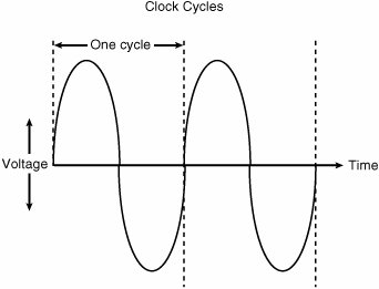
EAN: 2147483647
Pages: 283