Motherboard Components
| A modern motherboard has several components built in, including various sockets, slots, connectors, chips, and so on. This section examines the components found on a typical motherboard. Most modern laptop motherboards have at least the following major components on them:
Most laptop motherboards also include integrated video, audio, networking, or other optional interfaces, depending on the individual board. Most of these standard components are discussed in the following sections. Processor Sockets/SlotsThe CPU in a laptop system can be soldered directly into the motherboard, installed via a mobile module (a circuit board containing the CPU and other components), or plugged in via a socket similar to that of desktop systems. Most modern systems have the processor installed in a socket directly, allowing future replacement and even limited upgrades. Processors earlier than the Pentium III and Athlon were usually soldered in or installed via various mobile module designs, greatly limiting interchangeability. Table 5.4 shows the designations for the various processor sockets/slots used in laptop systems and lists the chips designed to plug into them.
Note that some laptops use desktop processors, so they might use desktop processor sockets. Most, however, use specific processors and sockets designed for mobile use. Just because a processor fits into a particular socket does not mean that it will function. For example, versions of the Celeron, Pentium III, Pentium 4, and Pentium M all plug into an mPGA479M socket, but only the one that the system is designed for will work; in fact, plugging in the wrong one could cause damage. Despite having similar pin counts and physical arrangements, the actual pinouts vary among the different processors. ChipsetsWe can't talk about modern motherboards without discussing chipsets. The chipset is the motherboard; therefore, any two boards with the same chipsets are functionally identical. The chipset contains the processor bus interface (called the front-side bus, or FSB), memory controllers, bus controllers, I/O controllers, and more. All the circuits of the motherboard are contained within the chipset. If the processor in your PC is like the engine in your car, the chipset represents the chassis. It is the framework in which the engine rests and is its connection to the outside world. The chipset is the frame, suspension, steering, wheels and tires, transmission, driveshaft, differential, and brakes. The chassis in your car is what gets the power to the ground, allowing the vehicle to start, stop, and corner. In the PC, the chipset represents the connection between the processor and everything else. The processor can't talk to the memory, video processor, expansion cards, devices, and so on without going through the chipset. The chipset is the main hub and central nervous system of the PC. If you think of the processor as the brain, the chipset is the spine and the central nervous system. Because the chipset controls the interface or connections between the processor and everything else, the chipset ends up dictating which type of processor you have; how fast it will run; how fast the buses will run; the speed, type, and amount of memory you can use; and more. In fact, the chipset might be the single most important component in your system, possibly even more important than the processor. I've seen systems with faster processors be outperformed by systems with slower processors but a better chipset, much like how a car with less power might win a race through better cornering and braking. When deciding on a system, I start by choosing the chipset because the chipset decision then dictates the processor, memory, I/O, and expansion capabilities. Chipset EvolutionWhen IBM created the first PC motherboards, it used several discrete (separate) chips to complete the design. Besides the processor and optional math coprocessor, many other components were required to complete the system. These other components included items such as the clock generator, bus controller, system timer, interrupt and DMA controllers, CMOS RAM and clock, and keyboard controller. Additionally, many other simple logic chips were used to complete the entire motherboard circuitplus, of course, things such as the actual processor, math coprocessor (floating-point unit), memory, and other parts. Table 5.5 lists all the primary chip components used on the original PC/XT and AT motherboards.
Although the specifications shown here are for PC/XT and AT systems, keep in mind that, in that day, portables were not really laptops. Instead, they mimicked desktop technology almost exactly. In essence, a portable was a desktop with a handle. By the time laptops really came around, chipsets were already invented and in use in desktops as well. In addition to the processor/coprocessor, a six-chip set was used to implement the primary motherboard circuit in the original PC and XT systems. IBM later upgraded this to a nine-chip design in the AT and later systems, mainly by adding more interrupt and DMA controller chips and the nonvolatile CMOS RAM/real-time clock chip. All these motherboard chip components came from Intel or an Intel-licensed manufacturer, except the CMOS/clock chip, which came from Motorola. Building a clone or copy of one of these IBM systems required all these chips, plus many smaller discrete logic chips to glue the design together, totaling 100 or more individual chips. This kept the price of a motherboard high and left little room on the board to integrate other functions. In 1986, a company called Chips and Technologies introduced a revolutionary component called the 82C206the main part of the first PC motherboard chipset. This was a single chip that integrated into it all the functions of the main motherboard chips in an AT-compatible system. This chip included the functions of the 82284 clock generator, 82288 bus controller, 8254 system timer, dual 8259 interrupt controllers, dual 8237 DMA controllers, and even MC146818 CMOS/clock chip. Besides the processor, virtually all the major chip components on a PC motherboard could now be replaced by a single chip. Four other chips augmented the 82C206 acting as buffers and memory controllers, thus completing virtually the entire motherboard circuit with five total chips. Chips and Technologies called this first chipset the CS8220 chipset. Needless to say, this was a revolutionary concept in PC motherboard manufacturing. Not only did it greatly reduce the cost of building a PC motherboard, but it also made designing a motherboard much easier. The reduced component count meant that the boards had more room for integrating other items formerly found on expansion cards. Later, the four chips augmenting the 82C206 were replaced by a new set of only three chips, and the entire set was called the New Enhanced AT (NEAT) 82C836 Single Chip AT (SCAT) chipset, which finally condensed all the chips in the set to a single chip. Since then, many chipset manufacturers have come and gone, and after a major shakeup in the chipset industry, only Intel, AMD, VIA Technologies, SiS, and ALi make motherboard chipsets. Intel has come to dominate the chipset market for systems using Intel processors, although other companies such as VIA Technologies, SiS, and ALi also make chipsets supporting Intel processors. AMD has developed its own chipsets for the K6 and Athlon family of processors, but it now emphasizes third-party chipset developers to support its products. Today VIA Technologies is the leading developer of AMD Athlon/Athlon XP/Duron chipsets. The popularity of AMD processors has also encouraged SiS, NVIDIA, and the ALi Corporation to develop chipsets for both Intel- and AMD-based systems. It is interesting to note that the original PC chipset maker, Chips and Technologies, survived by changing course to design and manufacture video chips, and found a niche in that market specifically for laptop video chipsets. Chips and Technologies was subsequently bought out by Intel in 1998 as a part of Intel's video strategy. Intel ChipsetsYou can't talk about chipsets today without discussing Intel because it currently owns the vast majority of the chipset market, especially for Intel processorequipped mobile systems. Now as Intel develops new processors, it develops chipsets and motherboards simultaneously, which means that they can be announced and shipped in unison. This eliminates the delay between introducing new processors and waiting for motherboards and systems capable of using them, which was common in the industry's early days. For the consumer, this means no waiting for new systems. Since the original Pentium processor in 1993, you have been able to purchase ready-made systems on the same day a new processor is released. Starting with the 486 in 1989, Intel began a pattern of numbering its chipsets as follows:
The chipset numbers listed here are abbreviations of the actual chipset numbers stamped on the individual chips. For example, one of the popular laptop Pentium II/III chipsets was the Intel 440BX chipset, which consisted of two components: the 82443BX North Bridge and the 82371EX South Bridge. Likewise, the 845 chipset supports the Mobile Pentium 4 and consists of two main parts, including the 82845 memory controller hub (MCH, which replaces the North Bridge) and an 82801CAM I/O controller hub (ICH3-M, which replaces the South Bridge). By reading the logo (Intel or others) as well as the part number and letter combinations on the larger chips on your motherboard, you can quickly identify the chipset your motherboard uses. Intel has used two distinct chipset architectures: a North/South Bridge architecture and a newer hub architecture. All its more recent 800 series chipsets use the hub architecture, while the newer 900 series use PCI Express. In the 900 series, the connection between the North Bridge (memory controller hub) and South Bridge (I/O controller hub) is a new interface called Direct Media Interface (DMI), which is basically a modified PCI Express x4 interface supporting a throughput of 1GBps in each direction simultaneously. AMD Athlon/Duron ChipsetsAMD took a gambleone that was ultimately successfulwith its Athlon family of processors (Athlon, Athlon XP, Athlon MP, and the now-discontinued Duron). With these processors, AMD decided for the first time to create a chip that was Intel compatible with regard to software but not directly hardware or pin compatible. Whereas the K6 series would plug into the same Socket 7 that Intel designed for the Pentium processor line, the AMD Athlon and Duron would not be pin compatible with the Pentium II/III and Celeron chips. This also meant that AMD could not take advantage of the existing chipsets and motherboard designs when the Athlon and Duron were introduced; instead, AMD would have to either create its own chipsets and motherboards or find other companies that would. Although it would take some time for AMD to put its processors and chipset designs into laptops systems, AMD took its first step into the world of chipsets when it bootstrapped the market by introducing its own chipset, referred to as the AMD-750 chipset (code-named Irongate). The AMD 750 chipset consists of the 751 system controller (North Bridge) and the 756 peripheral bus controller (South Bridge). More recently, AMD introduced the AMD-760 chipset for the Athlon/Duron processors, which is the first major chipset on the market that supports DDR SDRAM for memory. It consists of two chips: the AMD-761 system bus controller (North Bridge) and the AMD-766 peripheral bus controller (South Bridge). Although AMD no longer puts much emphasis on chipset sales, its pioneering efforts have inspired other companies, such as VIA Technologies, NVIDIA, and SiS, to develop chipsets specifically designed for the Slot A and current Socket A and Socket 754 processors from AMD. This has enabled the motherboard companies to make a variety of boards supporting these chips and the Athlon processors, taking a fair amount of market share away from Intel in the process. North/South Bridge ArchitectureMost older chipsets are broken into a multitiered architecture incorporating what are referred to as North and South Bridge components, as well as a Super I/O chip:
The North Bridge is sometimes referred to as the PCI/AGP controller (PAC). It is essentially the main component of the motherboard and is the only motherboard circuit besides the processor that normally runs at full motherboard (processor bus) speed. Most modern chipsets use a single-chip North Bridge; however, some of the older ones actually consisted of up to three individual chips to make up the complete North Bridge circuit. The South Bridge is the lower-speed component in the chipset and has always been a single individual chip. The South Bridge is a somewhat interchangeable component, in that different chipsets (North Bridge chips) often are designed to use the same South Bridge component. This modular design of the chipset allows for lower cost and greater flexibility for motherboard manufacturers. The South Bridge also typically contains dual ATA interfaces, several USB interfaces, and even the CMOS RAM and real-time clock functions. The South Bridge contains all the components that make up the ISA bus, including the interrupt and DMA controllers. The third motherboard component, the Super I/O chip, is connected to the 8MHz ISA bus and contains all the standard peripherals that are built in to a motherboard. For example, most Super I/O chips contain the serial ports, parallel port, floppy controller, and keyboard/mouse interface. Figure 5.1 shows a typical North/South Bridge architecture using the 440BX chipset. This was the most popular chipset and system architecture for late Pentium II or early Pentium III laptops. Figure 5.1. Typical 440BX chipset laptop motherboard block diagram. More recent motherboards using North/South Bridge chipset designs often incorporate a Super South Bridge, which incorporates the South Bridge and Super I/O functions into a single chip. Intel Hub ArchitectureThe newer 800-series chips from Intel use a hub architecture in which the former North Bridge chip is now called a memory controller hub (MCH) and the former South Bridge is called an I/O controller hub (ICH). Instead of being connected through the PCI bus as in a standard North/South Bridge design, they are connected via a dedicated hub interface that is twice as fast as PCI. The hub design offers several advantages over the conventional North/South Bridge design:
This hub interface design allows for a much greater throughput for PCI devices because no South Bridge chip (also carrying traffic from the Super I/O chip) is hogging the PCI bus. Because of bypassing PCI, hub architecture also enables greater throughput for devices directly connected to the I/O controller hub (formerly the South Bridge), such as the new higher-speed ATA-100/133, Serial ATA, and USB 2.0 interfaces. The hub interface design is also very economical, at only 8 bits wide. Although this seems too narrow to be useful, there is a reason for the design. Because the interface is only 8 bits wide, it uses only 15 signals, compared to the 64 signals required by the 32-bitwide PCI bus interface used by North/South Bridge chip designs. The lower pin count means that less circuit routing exists on the board, less signal noise and jitter occur, and the chips themselves have fewer pins, making them smaller and more economical to produce. Although it transfers only 8 bits at a time, the hub interface executes four transfers per cycle and cycles at 66MHz. This gives it an effective throughput of 4 x 66MHz x 1 byte = 266MBps. This is twice the bandwidth of PCI, which is 32 bits wide but runs only one transfer per 33MHz cycles, for a total bandwidth of 133MBps. So, by virtue of a very narrowbut very fastdesign, the hub interface achieves high performance with less cost and more signal integrity than with the previous North/South Bridge design. The MCH interfaces between the high-speed processor bus (800/533/400/133/100/66MHz) and the hub interface (66MHz) and AGP bus (533/266/133/66MHz), whereas the ICH interfaces between the hub interface (66MHz) and the ATA(IDE) ports (66/100MHz) and PCI bus (33MHz). The ICH also includes a new Low Pin Count (LPC) bus, consisting basically of a stripped 4-bitwide version of PCI designed primarily to support the motherboard ROM BIOS and Super I/O chips. Because it uses the same 4 signals for data, address, and command functions, only 9 other signals are necessary to implement the bus, for a total of only 13 signals. This dramatically reduces the number of traces connecting the ROM BIOS chip and Super I/O chips in a system, compared to the 96 ISA bus signals necessary for older North/South Bridge chipsets that used ISA as the interface to those devices. The LPC bus has a maximum bandwidth of 16.67MBps, which is faster than ISA and more than enough to support devices such as ROM BIOS and Super I/O chips. Figure 5.2 shows a typical hub interface architecture using the 855PM chipset. This is the most popular chipset and system architecture for Pentium M laptops, and it represents a modern state-of-the-art system design. Figure 5.2. Typical 855PM chipset laptop motherboard block diagram. Intel DMI ArchitectureThe 900 series chipsets from Intel have abandoned the hub interface in favor of a new interface called Direct Media Interface (DMI). DMI is basically a modified PCI Express x4 (4-lane) interface supporting a throughput of 1GBps in each direction simultaneously. Being a dedicated connection between the chips in the chipset, DMI incorporates all of the same advantages of the former hub interface, along with a significantly higher-speed interconnection. Figure 5.3 shows where DMI fits into the 915 chipset between the 915PM memory controller hub (MCH) and the ICH6-M I/O controller hub. Figure 5.3. Typical 915PM chipset laptop motherboard block diagram.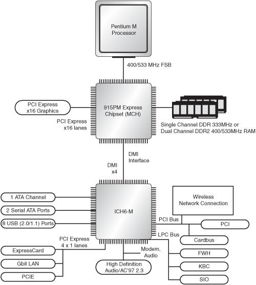 Note Although other chipset makers typically use the North Bridge/South Bridge nomenclature for their chipsets, several have developed high-speed connections similar to Intel's hub architecture and DMI. For example, most of VIA's recent chipsets use the V-Link hub architecture, which provides a dedicated 266MHz bus between the North and South Bridge chips. The high-speed HyperTransport bus between the North and South Bridges originally developed by AMD has been licensed by chipset vendors such as NVIDIA, VIA, and ALi Corporation; SiS's MuTIOL Connect is used by recent SiS chipsets. Other High-Speed North-South Bridge ConnectionsIntel is not alone in replacing the slow PCI bus connection between North and South Bridgetype chips with faster architectures that bypass the PCI bus. Other companies introducing high-speed chipset interconnects include these:
It's worth noting that although these chipsets were originally deployed in desktop systems, their appearance in laptop systems was simultaneous, in most cases. Although the terms North Bridge and South Bridge continue to be used for chipsets using V-Link, MuTIOL, A-Link, or HyperTransport interconnects between these chipset components, these chipsets really use a hub-based architecture similar to that of Intel 8xx-series chipsets and receive corresponding boosts in performance as a consequence. Chipset ProfilesTo get the most out of any processor, you must use a high-performance chipset. As when shopping for a desktop system, you should be aware of what chipset is used in the portable computer you plan to buy and whether it fully supports the capabilities of the processor and the system's other components. The following sections describe the most popular chipsets found in portable systems using Pentium and newer processors. Mobile Pentium ChipsetIntel had only a single mobile-specific chipset for Pentium systems. However, many laptops used desktop processors and chipsets, despite the drawbacks in power consumption. Intel 430MXIntel introduced the 430MX in October 1995, designed to support the Pentium and Pentium MMX processors. The 430MX mobile chipset was similar in architecture and performance to the then-popular 430FX desktop socket 7 chipset, although it is important to note that the processor was normally soldered in, not socketed in mobile designs of that time. Most Pentium-based laptop and portable systems used this chipset from the mid- to late-1990s. The 82430MX consisted of four total chips, including a three-chip North Bridge: the 82437MX system controller and two 82438MX data path chips, and the 82371MX MPIIX (Mobile PCI I/O IDE Accelerator) South Bridge. These components are in Quad Flat Pack (QFP) and Thin Quad Flat Pack (TQFP) packaging, to allow thin and light designs. Notable features for the 430MX include these:
To provide extended battery life for use in portable systems, the 430MX featured power-management functions not normally found in desktop chipsets:
The 430MX PCIset was originally priced at $32.50 (U.S.) in 10,000-unit quantities and was by far the most popular chipset used in Pentium- and Pentium MMX processorbased portables. Pentium II/III ChipsetsIntel, VIA, and others offered several chipsets designed for mobile Pentium II and III processors and systems. Some, such as the 440BX, were originally designed for desktop use and then later were adapted for mobile processors. Others, such as the 440MX, were specifically designed for mobile use. Intel 440BXThe Intel 440BX chipset was introduced in April 1998 and was the first chipset to run the processor host bus (often called the front-side bus, or FSB) at 100MHz. The 440BX was designed specifically to support the faster Pentium II/III processors at 350MHz and higher. This chipset was the first Pentium II/III chipset for laptop systems as well. The main change from previous chipsets is that the 440BX chipset improves performance by increasing the bandwidth of the system bus from 66MHz to 100MHz. Because the chipset can run at either 66MHz or 100MHz, it allows one basic motherboard design to support all Pentium II/III processor speeds based on either the 66MHz or 100MHz processor bus. Here are the Intel 440BX highlights:
The Intel 440BX consists of a single North Bridge chip called the 82443BX host bridge/controller, which is paired with an 82371EB PCI-ISA/IDE Xcelerator (PIIX4E) South Bridge chip. The South Bridge adds support for the advanced configuration and power interface (ACPI) specification version 1.0. The 440BX is also used in mobile module versions of the Pentium II and III processors. In a mobile module design, the chipset's two halves, called the North Bridge and the South Bridge, are located on the mobile module and the motherboard, respectively. The 440BX was the most popular chipset for portables of the late 1990s, which were based on the Pentium II and III and Celeron processors. Intel 440MXThe 440MX chipset is essentially a 440BX North Bridge and PIIX4E South Bridge combined into a single chip. In addition to consolidating the two chips into one, the 440MX adds integrated AC'97 (audio codec 1997) audio and modem support, which provides a built-in sound card and modem comparable to those of PCI-based cards. The 440MX is identical to the 440BX, except for the following features:
Intel 440ZXThe 440ZX-66M is a low-cost version of the 440BX designed specifically to support the low-end mobile Celeron processors based on Pentium II and III designs. The main difference from the 440BX is that the 440ZX is limited to a 66MHz processor front-side bus (FSB). VIA PN133The VIA PN133 is a Pentium III processor chipset combining an integrated Savage4 graphics core with 133MHz processor bus and 133MHz SDRAM support. The PN133 is ideally suited for thin and light or entry-level laptop systems. The main features of the PN133 include the following:
Built-in high performance 2D/3D graphics, flexible 66/100/133MHz system bus settings, support for PC100/133 SDRAM, and multiple power saving modes make the VIA ProSavage PN133 (code-named Twister) the ideal integrated SMA chipset for the Intel Pentium III, Intel Celeron, and VIA C3 processor laptops. Intel 815EMThe 815EM chipset is a mainstream laptop Pentium III/Celeron chipset with an economical integrated AGP 2x video controller that shares system RAM. Similar to the other 8xx-series chipsets from Intel, the 815EM (82815EM GMCH2-M) uses Intel's hub architecture, providing a 266MBps connection between the two main chipset components. This chipset does not share the PCI bus like the older North/South Bridge designs do. The 815EM supports the following features:
The 815EM uses the ICH2-M (82801BAM) I/O controller hub, which is most notable for providing ATA-100 support. Although few drives can really take advantage of this much throughput, in any case there won't be a bottleneck there. The other notable feature is having two USB 1.1 controllers and four total USB ports on board. This allows double the standard USB 1.1 performance by splitting up devices over the two ports, and can allow up to four connections before a hub is required. A companion chip called the 82807AA video controller hub (VCH) connects directly to the digital video-out port on the GMCH2-M, enabling low-voltage differential signaling (LVDS) for LCD panel support with the 815EM integrated graphics. Another important feature of the 815EM is the integration of a fast Ethernet controller directly into the chipset. The integrated LAN controller works with a physical-layer component that includes the following:
These physical-layer components can be placed directly on the motherboard (additional chips) or can be installed via an adapter that plugs into a Mini PCI slot. The 815EM chipset was a popular Pentium IIIclass chipset for the mainstream laptop market and was essentially designed to replace the venerable 440Bx chipset. Intel 830M/MG/MPThe 830 chipset family is the last chipset Intel released for the Mobile Intel Pentium III and Celeron processor-based laptops. The 830 chipset increases the processor bus speed to 133MHz and also supports PC133 SDRAM. The 830 chipset comes in three versions:
The 830 chipset family also supports the following:
Pentium 4 ChipsetsIntel introduced several chipsets for use with Mobile Pentium 4-M and Mobile Pentium 4 processors. Some, such as the 845MP/MZ, were simply mobile versions of desktop chipsets. Others, such as the 852 family, were specifically designed for mobile use. Intel 845MP/MZThe 845M chipset family is designed for low-end Mobile Pentium 4 systems. The 845M chipset family includes two versions, with the following differences:
Both chips in the 845M chipset family (82845MP/MZ memory controller hub) support the following features:
Intel 852PM/GM/GMEThe 852 chipset family is a mainstream Mobile Pentium 4 chipset with advanced mobile power management, support for DDR SDRAM memory, and optional integrated graphics and/or AGP 4x support. The most basic member of the family is the 852G, which supports a 400MHz processor bus, up to 1GB of DDR200/266 (PC1600/PC2100) memory, as well as an integrated Intel Extreme Graphics AGP 2x video processor with support for dual independent displays and integrated low-voltage differential signaling (LVDS) with up to SXGA+ (1400x1050) LCD resolution. The 82852GM (MCH) includes the following:
The 852GME includes everything from the 852G and adds this:
The 852GME chipset is the same as the 852G, except that it supports the faster 533MHz Mobile Pentium 4 processor bus and up to 2GB of high-speed DDR266/333 (PC2100/PC2700) memory. The 852GME also includes an upgraded Intel Extreme Graphics/2 AGP 2x video processor with support for dual independent displays and integrated LVDS, with up to UXGA+ (1600x1200) LCD resolution. The integrated video processors built in to the 852G and 852GME dynamically share the main system RAM (no separate video RAM is used). The integrated 2x video with shared RAM results in a less expensive system than one using a third-party AGP 4x video processor with discrete video RAM, but with lower video performance as well. Most higher-performance laptops preferred to use a chipset without integrated video and instead build the equivalent of a video card on the motherboard, complete with a discrete video processor, video RAM, and video BIOS. In most laptops, the only difference between the built-in video and a separate video card (as in a desktop system) is that the built-in video card merely shares real estate with the rest of the motherboard. The 852PM chipset is the same as the 852GME (faster 533MHz processor bus and up to 2GB of high-speed DDR266/333 [PC2100/PC2700] memory), but it lacks the integrated video. Instead, an AGP 4x interface is included for connecting to third-party video processors. This makes the 852PM the best choice for high-performance mobile Pentium 4 systems. Pentium M ChipsetsIntel 855PM/GMThe Intel 855 chipset family is designed to support the 400MHz bus versions of the Pentium M and Celeron M mobile processors and is part of Intel's Centrino Mobile Technology platform when combined with an Intel wireless networking solution (see Figure 5.2). The combination of the 855 chipset and a Pentium M or Celeron M processor results in a powerful mobile system with low overall power consumption. The 855PM is a standard memory controller hub with AGP 4x support for a discrete video processor and video RAM, while the 855GM version adds an integrated video processor that shares system RAM. The 855PM includes the following features:
The 855GM includes everything from the 855PM and also adds an Integrated Intel Extreme Graphics/2 AGP 2x video processor with support for dual independent displays and integrated low-voltage differential signaling (LVDS), with up to UXGA+ (1600x1200) LCD resolution. Intel 915 Express Chipset FamilyThe Intel 915 mobile chipset family (code-named Alviso) was introduced in January 2005 and includes the 915PM/GM/GMS and 910GML. These chipsets are designed to support the Pentium M and Celeron M mobile processors in both 400MHz and 533MHz bus versions (dependent on the specific chipset), and are part of Intel's second generation Centrino Mobile Technology platform (codenamed Sonoma) when combined with an internal Intel wireless networking solution. The combination of the 915 chipset and a Pentium M or Celeron M processor results in a powerful mobile system with low overall power consumption. The 915 chipset supports up to 2GB of dual-channel DDR2 system memory, which allows for a significant increase in peak memory bandwidth and power benefits over the single-channel DDR that the 855 chipset supported. The 915 chipset also supports PCI Express bus architecture, which means that laptops using this chipset will have ExpressCard as well as CardBus sockets for expansion cards. Finally, the 915 chipset supports Intel High Definition Audio (HDA), which is an enhanced audio specification for high-quality surround-sound audio suitable for home theater. The 915PM is a standard memory controller hub with PCI Express x16 support for a separate video processor and video RAM, while the 915GM version adds an integrated video processor that shares system RAM. The integrated video in the 915GM is the Intel Graphics Media Accelerator 900, which has about twice the graphics performance of the integrated video in the older 855GM chipset. The 915 chipset family features include
There are four different chipsets in the family; the 915PM is the one that will be used in the highest-performance systems since it does not include built-in graphics but is instead designed to connect to a discrete PCI Express x16 graphics controller. The 915GM is the same chipset as the 915PM except that it does include the highest-performance version of Intel's GMA (Graphics Media Accelerator) integrated graphics technology. The 915GMS and 910GML are designed for smaller and lower-cost systems, and lack some of the features of the other chipsets in the family. Table 5.6 highlights the specific differences between all of the 915 family chipsets.
The 915 chipset includes either the 915PM/GM/GMS or 910GML memory controller hub (MCH) combined with the 82801FBM ICH6-M I/O controller hub (ICH). AMD Processor ChipsetsLike most Intel chipsets, chipsets designed for use with AMD processors usually appeared in desktops first. Eventually (and often simultaneously), they were also implemented in laptop systems. AMD-760The AMD-760 chipset is a highly integrated system logic solution that delivers enhanced performance for the AMD Athlon processor and other AMD Athlon system bus-compatible processors. The AMD-760 chipset consists of the AMD-761 system controller in a 569-pin plastic ball-grid array (PBGA) package and the AMD-766 peripheral bus controller in a 272-pin PBGA package. The AMD-761 system controller features the AMD Athlon system bus, DDR SDRAM system memory controller, accelerated graphics port (AGP 4X) controller, and Peripheral Component Interconnect (PCI) bus controller. The AMD-766 peripheral bus controller features four primary blocks (PCI-to-ISA/LPC bridge, OHCI USB host controller, EIDE UDMA-33/66/100 controller, and system management logic), each with independent access to the PCI bus, a complete set of PCI interface signals and state machines, and the capability of working independently with separate devices. VIA Apollo KN133The VIA KN133 is designed to support the AMD Mobile Athlon and Mobile Duron processors, and includes integrated 2D/3D graphics, 200/266MHz processor bus settings, support for PC100/133 SDRAM and multiple power-saving modes. The main features of the KN133 include the following:
VIA KN266The VIA KN266 chipset for AMD Athlon and Duron mobile processors includes an integrated S3 ProSavage8 2D/3D Graphics engine, plus support for up to 4GB of DDR266 (PC2100) memory. The integrated S3 ProSavage8 graphics incorporate AGP 8x bandwidth and DVD motion compensation, and are optimized for use with Windows XP. The integrated video uses shared memory architecture (SMA, also called unified memory architecture or UMA), which means that it shares the main system RAM instead of using discrete video RAM. The integrated graphics offer lower system power consumption and save motherboard real estate, thus enabling thinner and lighter form factors. The KN266 uses VIA's V-Link hub architecture, which provides a dedicated 266MBps bus between the North and South Bridge (see Figure 5.4). This is similar to the hub architecture pioneered in the Intel 8xx chipsets. The KN266 also includes an integrated AC'97 audio/modem support for ATA-100 and up to six USB 1.1 ports. Other options include an integrated 3Com networking interface. Figure 5.4. VIA KN266 chipset block diagram. Features of the KN266 include these:
| ||||||||||||||||||||||||||||||||||||||||||||||||||||||||||||||||||||||||||||||||||||||||||||||||||||||||||||||||||||||||||||||||||||||||||||||||||||||||||||||||||||||||||||||||||||||||||||||||||||||||||||||||||||||||||||||||||||||||||||||||||||||||

EAN: 2147483647
Pages: 180