7.10 The Composite Digital Parallel Interface
| | ||
| | ||
| | ||
7.10 The Composite Digital Parallel Interface
When composite video is to be digitized, the input will be a single waveform having spectrally interleaved luminance and chroma. Any sampling rate allowing sufficient bandwidth would convey composite video from one point to another. However, if processing in the digital domain is contemplated, there will be less choice.
In the composite digital colour processor it will be necessary to decode the composite signal, which will require some kind of digital filter. Whilst it is possible to construct filters with any desired response, it is a fact that a digital filter whose response is simply related to the sampling rate will be much less complex to implement. This is the reasoning that led to the near universal use of four times subcarrier sampling rate. Figure 7.17 shows the spectra of PAL and NTSC sampled at 4 — F sc . It will be evident that there is a considerable space between the edge of the baseband and the lower sideband. This allows the anti-aliasing and reconstruction filters to have a more gradual cut-off, so that ripple in the passband can be reduced. This is particularly important for composite digital recorders , since they are digital devices in an analog environment, and signals may have been converted to and from the digital domain many times in the course of production. A subcarrier multiple sampling clock is easily obtained by gating burst to a phase-locked loop. In NTSC there is no burst swing, whereas at 4 F sc , the burst swing of PAL moves burst crossings by exactly one sample period and so the phase relationship between burst crossings and 4 F s , clock is unaffected by burst swing.
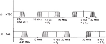
Figure 7.17: The spectra of NTSC at (a) and of PAL at (b) where both are sampled at four times the frequency of their respective subcarriers. This high sampling rate is unnecessary to satisfy sampling theory, and so both are oversampled systems. The advantages are in the large spectral gap between baseband and sideband which allows a more gentle filter slope to be employed, and in the relative ease of colour processing at a sampling rate related to subcarrier.
In NTSC, siting of samples along the line is affected by ScH phase. In PAL, the presence of the 25 Hz component of subcarrier means that samples are not in exactly the same place from one line to the next . The columns lean over slightly such that at the bottom of a field there is a displacement of two samples with respect to the top.
Composite digital samples at four times subcarrier frequency, and so there will be major differences between the PAL and NTSC standards. It is not possible to transmit digitized SECAM. Whilst the component interface transmits only active lines and special sync patterns, the composite interfaces carry the entire composite waveform syncs, burst and active line. Although ancillary data may be placed in sync tip, the rising and falling sync edges must be present. In the absence of ancillary data, the data on the parallel interface is essentially the continuous stream of samples from a convertor which is digitizing a normal analog composite signal. Virtually all that is necessary to return to the analog domain is to strip out ancillary data and substitute sync tip values prior to driving a DAC and a filter. One of the reasons for this different approach is that the sampling clock in composite video is subcarrier locked. The sample values during sync can change with ScH phase in NTSC and PAL and change with the position in the frame in PAL due to the 25 Hz component. It is simpler to convey sync sample values on the interface than to go to the trouble of recreating them later.
The instantaneous voltage of composite video can go below blanking on dark saturated colours, and above peak white on bright colours. As a result the quantizing ranges need to be stretched in comparison with component in order to accommodate all possible voltage excursions. Sync tip can be accommodated at the low end and peak white is some way below the end of the scale. It is not so easy to determine when overload clipping will take place in composite as the sample sites are locked to subcarrier. The degree of clipping depends on the chroma phase. When samples are taken either side of a chroma peak, clipping will be less likely to occur than when the sample is taken at the peak. Advantage is taken of this phenomenon in PAL as the peak analog voltage of a 100% yellow bar goes outside the quantizing range. The sampling phase is such that samples are sited either side of the chroma peak and remain within the range.
The PAL and NTSC versions of the composite digital interface will be described separately. The electrical interface is the same as for a digital component.
7.10.1 PAL Interface
The quantizing range of digital PAL is shown in Figure 7.18 8 . Blanking level is at 256 10 (64 10 ) and sync tip is the lowest allowable code of 4(1) as 0 is reserved for digital synchronizing. Peak white is 844 10 (211 10 ).
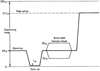
Figure 7.18: The composite PAL signal fits into the quantizing range as shown here. Note that there is sufficient range to allow the instantaneous voltage to exceed that of peak white in the presence of saturated bright colours. Values shown are decimal equivalents in a tenor eight-bit system. In a ten-bit system the additional two bits increase resolution, not magnitude, so they are below the radix point and the decimal equivalent is unchanged. PAL samples in phase with burst, so the values shown are on the burst peaks and are thus also the values of the envelope.
In PAL, the composite digital interface samples at 4 — F sc , with sample phase aligned with burst phase. PAL burst swing results in burst phases of 135 degrees, and samples are taken at these phases and at 45 degrees, precisely half-way between the U and V axes. This sampling phase is easy to generate from burst and avoids premature clipping of chroma. It is most important that samples are taken exactly at the points specified, since any residual phase error in the sampling clock will cause the equivalent of a chroma phase error when samples from one source are added to samples from a different source in a switcher. A digital switcher can only add together pairs of samples from different inputs, but if these samples were not taken at the same instants with respect to their subcarriers, the samples represent different vectors and cannot be added.
Figure 7.19 shows how the sampling clock may be derived. The incoming sync is used to derive a burst gate, during which the samples of burst are analysed. If the clock is correctly phased, the sampled burst will give values of 380 10 (95 10 ), 256 10 (64 10 ), 128 10 (32 10 ), 256 10 (64 10 ) repeated, whereas if a phase error exists, the values at the burst crossings will be above or below 256 10 (64 10 ). The difference between the sample values and blanking level can be used to drive a DAC that controls the sampling VCO. In this way any phase errors in the ADC are eliminated, because the sampling clock will automatically servo its phase to be identical to digital burst. Burst swing causes the burst peak and burst crossing samples to change places, so a phase comparison is always possible during burst. DC level shifts can be removed by using both positive and negative burst crossings and averaging the results. This also has the effect of reducing the effect of noise.
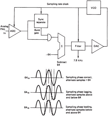
Figure 7.19: Obtaining the sample clock in PAL. The values obtained by sampling burst are analysed. When phase is correct, burst will be sampled at zero crossing and sample value will be 64 10 or blanking level. If phase is wrong, sample will be above or below blanking. Filter must ignore alternate samples at burst peaks and shift one sample every line to allow for burst swing. It also averages over several burst crossings to reduce jitter. Filter output drives DAC and thus controls sampling clock VCO.
In PAL, the subcarrier frequency contains a 25 Hz offset, and so 4 — F sc will contain a 100 Hz offset. The sampling rate is not h- coherent , and the sampling structure is not quite orthogonal. As subcarrier is given by:
F sc = 283.75 — F h + F v /2
the sampling rate will be given by:
F s = 1135 F h + 2 F v
This results in 709 379 samples per frame, and there will not be a whole number of samples in a line. In practice, 1135 sample periods, numbered 0 to 1134, are defined as one digital line, with an additional 2 sample periods per field which are included by having 1137 samples, numbered 0 to 1136, in lines 313 and 625. Figure 7.20(a) shows the sample numbering scheme for an entire line. Note that the sample numbering begins at 0 at the start of the digital active line so that the horizontal blanking area is near the end of the digital line and the sample numbers will be large. The digital active line is 948 samples long and is longer than the analog active line. This allows the digital active line to move with 25 Hz whilst ensuring the entire analog active line is still conveyed.
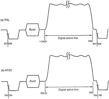
Figure 7.20: (a) Sample numbering in digital PAL. There are defined to be 1135 sample periods per line of which 948 are the digital active line. This is longer than the analog active line. Two lines per frame have two extra samples to compensate for the 25 Hz offset in subcarrier. NTSC is shown at (b). Here there are 910 samples per line of which 768 are the digital active line.
Since sampling is not h-coherent, the position of sync pulses will change relative to the sampling points from line to line. The relationship can also be changed by the ScH phase of the analog input. Zero ScH is defined as coincidence between sync and zero degrees of subcarrier phase at line 1 of field 1. Since composite digital samples on burst phase, not on subcarrier phase, the definition of zero ScH will be as shown in Figure 7.21, where it will be seen that two samples occur at exactly equal distances either side of the 50% sync point. If the input is not zero ScH, the samples conveying sync will have different values. Measurement of these values will allow ScH phase to be computed.
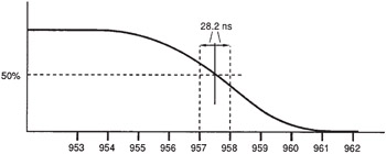
Figure 7.21: As PAL is sampled half-way between the colour axes, sample sites will fall either side of 50% sync at the zero ScH measurement line.
7.10.2 NTSC Interface
Although they have some similarities, PAL and NTSC are quite different when analysed at the digital sample level. Figure 7.22 shows how the NTSC waveform fits into the quantizing structure 9 . Blanking is at 240 14 (60 10 ) and peak white is at 800 10 (200 10 ), so that 1 IRE unit is the equivalent of 1.4 Q which could perhaps be called the DIRE. These different values are due to the different sync/vision ratio of NTSC. PAL is 7:3 whereas NTSC is 10:4.
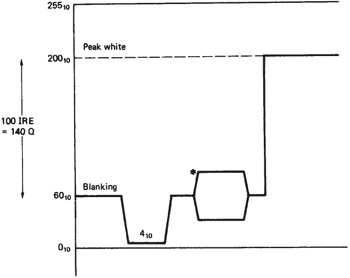
Figure 7.22: The composite NTSC signal fits into the quantizing range as shown here. Note that there is sufficient range to allow the instantaneous voltage to exceed peak white in the presence of saturated, bright colours. Values shown are decimal equivalents in an eight- or ten-bit system. In a ten-bit system the additional two bits increase resolution, not magnitude, so they are below the radix point and the decimal equivalent is unchanged. * Note that, unlike PAL, NTSC does not sample on burst phase and so values during burst are not shown here. See Figure 7.23 for burst sample details.
Subcarrier in NTSC has an exact half-line offset, so there will be an integer number of cycles of subcarrier in two lines. F sc is simply 227.5 — F h , and as sampling is at 4 — F sc , there will be 227.5 — 4 = 910 samples per line period, and the sampling will be orthogonal. Figure 7.20(b) shows that the digital active line consists of 768 samples numbered 0 to 767. Horizontal blanking follows the digital active line in sample numbers 768 to 909.
The sampling phase is chosen to facilitate encoding and decoding in the digital domain. In NTSC there is a phase shift of 123 degrees between subcarrier and the I axis. As burst is an inverted piece of the subcarrier waveform, there is a phase shift of 57 degrees between burst and the I axis. Composite digital NTSC does not sample in phase with burst, but on the I and Q axes at 57, 147, 237 and 327 degrees with respect to burst.
Figure 7.23 shows how this approach works in relation to sync and burst. Zero ScH is defined as zero degrees of subcarrier at the 50% point on sync, but the 57 degree sampling phase means that the sync edge is actually sampled 25.6 ns ahead of, and 44.2 ns after, the 50% point. Similarly, when the burst is reached, the phase shift means that burst sample values will be 46 10 , 83 10 , 74 10 and 37 10 repeating. The phase-locked loop that produces the sampling clock will digitally compare the samples of burst with the values given here. As the burst is not sampled at a zero crossing, the slope will be slightly less. The gain of the phase error detector will also be less, and more prone to burst noise than in the PAL process. The phase error will normally be averaged over several burst samples to overcome this problem.
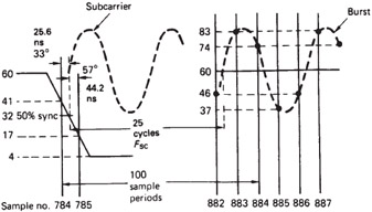
Figure 7.23: NTSC ScH phase. Sampling is not performed in phase with burst as in PAL, but on the I and Q axes. Since in NTSC there is a phase angle of 57 between burst and I , this will also be the phase at which burst samples should be taken. If ScH phase is zero, then phase of subcarrier taken at 50% sync will be zero, and the samples will be taken 33 before and 57 after sync; 25 cycles of subcarrier or 100 samples later, during burst, the sample values will be obtained. Note that in NTSC burst is inverted subcarrier, so sample 785 is positive, but sample 885 is negative.
| | ||
| | ||
| | ||
EAN: 2147483647
Pages: 120