Motherboards
|
| < Day Day Up > |
|
Contemporary motherboards support numerous processor bus frequencies within a wide frequency range. However, when comparing the parameters of motherboards, it is clear that different motherboards have not only different frequency values, but also different distributions within the frequency range. This occurs because contemporary motherboards use different frequency synthesizer chips.
Processor stability at high processor-bus frequencies is achieved by increasing of the processor supply voltage. When no built-in functions allow you to change the supply voltage, it is possible to use insulating varnish or another technique. This applies to almost any contemporary motherboard.
Currently, a processor-bus frequency above 250 MHz is not always a substantial advantage, although motherboards supporting even higher FSB values are announced regularly. No matter how advanced the motherboard might be, it is difficult to find other components (such as memory modules) capable of operating at such high frequencies. Besides this, not all high-frequency components of the motherboard would operate at such frequencies.
The memory-bus frequency, as well as the Accelerated Graphics Port (AGP) and Peripheral Component Interconnect (PCI) frequencies, are specified by the FSB frequency setting. Extremely high frequencies at these buses, depending on the motherboard architecture and chipset functionality, might cause hardware components to fail. This relates to RAM modules such as DIMM DDR SDRAM, video adapters (AGP or PCI), hard disks, and so on. However, many motherboards allow you to set fixed values of PCI/AGP frequencies (33/66 MHz) independent of the FSB frequency. These and other promising technologies are implemented in the architecture of the newest motherboard models, which appear on the market continually and in large quantities. Specialized chipsets, the basis of the motherboard architecture, ensure support of these new technologies.
Many chipsets and motherboard models are milestones in the history of computing.
Popular Chipsets
Intel Chipsets
Intel 440BX AGPset. The i440BX AGPset chipset is optimized for systems based on sixth-generation processors. Its architecture uses the Dual Independent Bus (DIB) with the Back Side Bus (BSB) interface, ensuring efficient operation of L2 cache memory (Fig. 4.25).
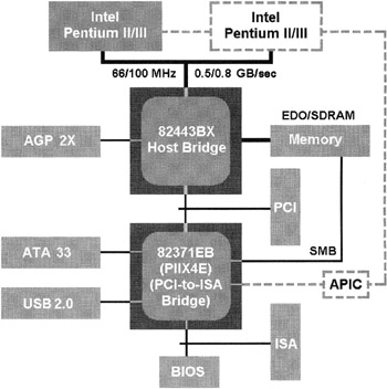
Figure 4.25: Structure of a computer based on the i440BX AGPset chipset
The i440BX AGPset supports FSB operation at 100 MHz. Dual-processor configurations are possible.
The support from FSB control functions built into the i440BX AGPset includes the following:
-
Intel Celeron, Pentium II, and Pentium III (Slot 1 and Socket 370) processors
-
Symmetric Multiprocessor (SMP) protocol for up to two processors
-
Buffering, hardware facilities for dynamic command execution, the pipelined data-transfer method, and input/output Advanced Programmable Interrupt Controller (APIC) tools
-
60 MHz, 66 MHz, and 100 MHz FSB frequencies (64-bit host bus GTL+)
Built-in memory controller support includes the following:
-
64-/72-bit memory bus (64 +8 ECC)
-
Extended Data Out (EDO) DRAM or SDRAM modules (60 MHz, 66 MHz, or 100 MHz) of 8 MB to 1 GB
-
3.3 V DIMM (Single/double density)
-
At 66 MHz: EDO DRAM (no worse than 60 nanoseconds) and SDRAM
-
At 100 MHz: SDRAM only (PC100)
-
Memory chips for 16- and 64-bit DRAM and up to four-sided DIMM (eight rows)
-
-
Parity control and ECC (for SDRAM only)
-
Unbuffered and registered SDRAM (x-1-1-1 at 66 MHz, and x-1-1-1 at 100 MHz)
-
DIMM plug-and-play through the Serial Presence Detect (SPD) mechanism using Intel's SMBus (System Management Bus) interface
The chipset doesn't support the coexistence of EDO DRAM and SDRAM. The memory-bus frequency always equals the FSB frequency (synchronous mode).
Built-in interface controllers and control tools support the following:
-
AGP Rev 1.0 (4/12/96) with 1X/2X modes (66/133 MHz, 3.3 V) and A6P sideband
-
PCI Rev. 2.1 (3.3 V and 5 V, 33 MHz, 32 bits)
-
Up to five PCI devices (in addition to the I/O bridge, PIIX4/PIIX4E)
-
Two Integrated Drive Electronics (IDE) ports (four IDE devices), and two Universal Serial Bus (USB) ports
-
System Management Bus (SMB), and bus mastering
-
PC '98 specification of Advanced Configuration and Power Interface (ACPI) power management for mobile and desktop computers
-
Wired for Management (WfM), Ultra DMA/33, and other devices
In systems based on i440BX, it is possible to use Ultra DMA/66 hard disks; however, they will operate in the Ultra DMA/33 mode.
The AGP and PCI bus frequencies are related to the processor-bus frequency. In the i440BX chipset, there are two coefficients relating AGP to FSB frequencies — 1:1 and 2:3. For the PCI bus, the value of this coefficient can be chosen from the following values — 1:2, 1:3, or 1:4. The last value is not supported by all motherboards; however, it is the one of the greatest interest to people who experiment with overclocking modes.
The i440BX AGPset chipset comprises two chips: 82443BX and 82371AB/EB. The 82443BX chip is known as the Host Bridge/Controller PCI AGP (PAC). The 82371AB/EB chip is the PCI-to-ISA/IDE Xcelerator (PIIX4/PIIX4E).
The problem caused by the lack of built-in Ultra DMA/66 and Ultra DMA/100 support in the i440BX chipset can be solved by installing an additional controller, implemented using specialized chips. For example, HPT366 or HPT370 from HighPoint Technologies can be used for this purpose.
In addition to the means of supporting Ultra DMA/66 and Ultra DMA/100 protocols, motherboard designers often add specialized chips for hardware monitoring, an essential architectural attribute of any contemporary system. This functionality is usually based on special chips such as Winbond W83782D.
Intel 815. Chipsets from the i815 line are based on Accelerated Hub Architecture (AHA). They are oriented toward high-performance computers with Pentium II/III processors (Slot 1 or Socket 370) and FSB frequencies of 66/100/133 MHz.
Built-in memory controller support includes the following:
-
Up to 512 MB PC100/133 SDRAM
-
Up to three DIMM modules
-
64-bit interface
Built-in tools support the following:
-
AGP 1X/2X/4X (integrated graphics based on the i752 chip, with up to six PCI)
-
Two (i815) or four (i815E) USB ports and two IDE ports (Ultra DMA/33/66 for 815, or Ultra DMA/33/66/100 for 815E)
-
LAN controller (i815E)
-
AC'97 audio with two (i815) or six (i815E) channels
-
ACPI power management, hardware monitoring, and other functions or devices
The i815 chipset comprises three chips: the 82815 Graphics and Memory Controller Hub (GMCH), the 82801AA I/O Controller Hub (ICH), and the 82802 Firmware Hub (FWH).
The i815E chipset comprises three chips: 82815 GMCH, 82801BA ICH2, and 82802 FWH.
Besides this, variants of i815 support Pentium III and Celeron processors based on the Tualatin core. These chipsets are marked as B-step.
Intel 845. Chipsets of this line are based on AHA (Fig. 4.26) and are intended for high-performance computers based on Pentium 4 processors (Socket 478 and Socket 423) with an FSB frequency of 100/133 MHz (400/533 MHz for data and 200/266 MHz for addresses).
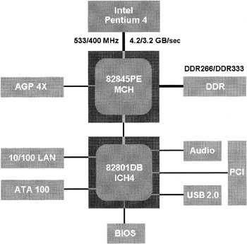
Figure 4.26: Structure of a computer based on the i845PE chipset
The FSB bus is a Quad Pumped Bus (QPB). At a 100 MHz clock frequency, it transmits data at 400 MHz and addresses at 200 MHz, which ensures a peak throughput of 3.2 GB/sec. At a clock frequency of 133 MHz, the data-transmission rate is 533 MHz, and the address rate is 266 MHz. In this mode, the peak throughput is 4.2 GB/sec. The bus supports 32-bit addressing, which ensures up to 4 GB RAM.
The built-in memory controller supports two types of memory: SDRAM (up to 3 GB with up to three DIMM modules, a 64-bit interface, PC100/133 SDRAM, etc.) or DDR SDRAM. The chipset version with DDR SDRAM is known as i845D.
The line of specialized i845 chipsets includes the following models: i845GL, i845GV, i845G, i845GE, i845E, and i845PE.
The most popular chipset from this line is i845PE, based on i845 and i845E.
The i845PE chipset is oriented toward systems with Pentium 4 or Celeron (Socket 478) processors with a 100/133 MHz FSB (QPB).
The built-in memory controller (Intel 82845PE MCH) supports the following:
-
DDR SDRAM and DDR266/333 modules
-
Maximum memory of 2 GB
-
64 MB, 128 MB, 256 MB, and 512 MB SDRAM chips
-
Unbuffered modules
-
Unregistered 184 pin without ECC DDR
The maximum data-transmission rate is 2.1/2.7 GB/sec with DDR266/333.
The built-in graphics controller supports one AGP device for AGP 2X/4X modes.
The second component of the chipset, the Intel 82801DB ICH4 chip, manages peripheral devices. This chip is included in the base set of the i845PE chipset.
Built-in tools of the base set support the following:
-
Two IDE channels with ATA 33/66/100/133 support (up to four IDE devices)
-
Three USB 2.0 controllers (six ports) and six PCI devices (32 bit/33 MHz)
-
AC'97 with support for six audio channels (20-bit AC-Link interface)
-
Integrated 10/100 Base-TX Ethernet controller
-
Low Pin Count (LPC), SMB, ACPI 2.0, and other functions and features
Because the i845PE chipset has considerable technological reserve, some motherboard manufacturers have released products that ensure support for a 200 MHz FSB (QPB).
Intel 850. Chipsets such as i850/i850E are based on AHA and are intended for high-performance computers with Pentium 4 (Socket 478 and Socket 423) processors operating at an FSB (QPB) clock frequency of 100/133 MHz (400/533 MHz for data and 200/266 MHz for addresses). The built-in memory controller supports two channels of up to 2 GB of Direct RDRAM, with up to four RIMM modules, PC800 RIMM, etc.
Built-in tools support the following:
-
AGP 1X/2X/4X, with up to six PCI or four USB ports
-
Two IDE ports with Ultra DMA/33/66/100 and a LAN controller
-
AC'97 audio with six channels
-
ACPI, hardware monitoring, and other features and functions
The i850 chipset comprises three chips: 82850 MCH, 82801BA ICH2, and 82802 FWH.
Intel 875. The i875P chipset, previously known as Canterwood, is oriented toward workstations and high-performance desktop computers (Fig. 4.27). It supports Pentium 4 processors with hyperthreading technology and manufactured using 0.13-micrometer technology. It is connected via the Socket 478 slot and has a FSB of the QPB type. The clock frequency can be 100 MHz, 133 MHz, or 200 MHz.
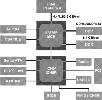
Figure 4.27: Structure of a computer based on the i875P chipset
The built-in Intel 82875P (MCH) controller of the QPB-type FSB supports a bus operating frequencies of 100/133/200 MHz, which ensures a data-transmission rate of 400/533/800 MHz.
The memory controller provides support for the following features:
-
Dual-channel and single-channel modes of DDR266/333/400 operation
-
Up to 4 GB of memory
-
128 MB, 256 MB, and 512 MB DDR SDRAM chips
-
Memory modules with or without ECC
In configurations that ensure ECC support in dual-channel mode, a 144-bit bus is used; without ECC, the bus is 128 bits.
Various frequency modes for processor buses and memory are listed in Table 4.27.
| FSB frequency (MHz) | Memory frequency (MHz) | Coefficient | Bandwidth (GB/sec) |
|---|---|---|---|
| 100 | 133 | 3:4 | 2.1 |
| 133 | 133 | 1:1 | 2.1 |
| 200 | 133 | 3:2 | 2.1 |
| 133 | 166 | 4:5 | 2.7 |
| 200 | 160 | 5:4 | 2.6 |
| 200 | 200 | 1:1 | 3.2 |
For synchronous operation of the DDR400 memory and 800 MHz bus, it is possible to implement the mode that ensures maximum performance of the memory subsystem: Intel Performance Acceleration Technology (PAT). In this mode, all delays related to synchronization are minimized.
The built-in graphics controller supports one 0.8/1.5 V AGP 3.0 device, operating in the AGP 8X mode.
Specific features of the MCH include implementation of a special interface (the CSA bus), which allows the implementation of Gigabit Ethernet. These features are ported from the ICH chip into MCH because of insufficient throughput of the local bus connecting MCH and ICH.
Control over peripheral devices is delegated to the second component of the chipset: ICH5, represented by Intel 82801EB chip. This chip is included in the base set of the i875P chipset.
Built-in control tools of this chip provide the following:
-
Two IDE channels with ATA 33/66/100 support (up to four IDE devices)
-
Two Serial ATA 150 ports, six USB 2.0 ports, and six PCI (32 bit/33 MHz)
-
AC'97 with support for three audio channel codecs
-
Integrated 10/100 Base-TX Ethernet controller
-
LPC, SMB, ACPI 2.0, and other tools and features
Besides Intel 82801EB, it is possible to use an extended version of ICH5: ICH5R. This extended version is represented by the Intel 82801ER chip. It differs from its predecessor by the presence of RAID 0 functionality, implemented according to the Intel RAID 0 technology.
Intel 865. The i865 chipset line, previously known as Springdale Canterwood, is oriented toward high-performance desktop PCs. It supports Intel Pentium 4 processors with hyperthreading technology and it is manufactured using the 0.13-micrometer process. It is connected via Socket 478 and supports the Quad Pumped Bus (QBP) type of FSB. Its clock frequency can be 100 MHz, 133 MHz, or 200 MHz (with a 400 MHz, 533 MHz, or 800 MHz data-transfer rate).
The PAT technology isn't officially supported.
The chipset supports the following features:
-
Dual-channel DDR266 memory (for any FSB frequency)
-
DDR333 (for 533/800 MHz) and DDR400 (for 800 MHz only)
-
AGP 8x and eight USB 2.0 ports
-
Intel's Communication Streaming Architecture (CSA) bus (for Intel Gigabit Ethernet chips)
-
Six PCI Busmaster devices
-
AC'97 codec(s) (20 bit)
-
Four IDE devices, with interface up to ATA 100, and two IDE devices with Serial ATA interface (with some limitations)
For the last two devices, it is possible to organize RAID 0, provided that the ICH5R South Bridge is used.
Via Technologies Chipsets
VIA Apollo Pro133A. The VIA Apollo Pro133A chipset supports Intel Celeron, Pentium II, and Pentium III (Slot 1 and Socket 370) processors. Among the most important characteristics of the Apollo Pro133A chipset is support for the following features:
-
66/100/133 MHz FSB, complying with the GTL+ standard
-
Synchronous and asynchronous bus operating modes, allowing operating modes of RAM modules to be set above the FSB frequency (+33 MHz)
-
Combined usage of SDRAM, Virtual Channel Memory (VCM) SDRAM, Enhanced SDRAM (ESDRAM), and EDO DRAM modules
-
Maximum memory of 2 GB and eight memory banks
PC133 specifications recommend a limit of three DIMM or six banks at 133 MHz. (The maximum memory in this configuration is 1.5 GB.)
Synchronous and pseudosynchronous bus operation modes allow the operating frequency of memory modules to be set above (+33 MHz) or below (-33 MHz) the FSB frequency.
The chipset also supports the following:
-
AGP 2.0 specifications, with the AGP 1X/2X/4X modes, and PC 2.1 specifications
-
Ultra DMA/33/66 modes for Enhanced Integrated Drive Electronics (EIDE) and USB ports
-
Keyboard and PS/2 mouse
-
RTC/CMOS within the VT82C694X chip
The Apollo Pro133A chipset comprises two chips: VT82C694X North Bridge and VT82C596B Mobile South Bridge.
In Apollo Pro133A, the VT82C686A chip can be used as a South Bridge. The chipset comprising VT82C694X and VT82C686A chips allows the creation of high-performance multimedia systems. All interactions with the processor, memory, and graphics are the responsibility of the North Bridge (VT82C694X). The South Bridge (VT82C686A) controls peripheral devices. The South Bridge chip includes support for Ultra DMA/66, AC'97 (implementation of a cheap built-in modem and sound card), two USB, and so on.
For support of the processors based on the Tualatin core, Via Technologies has released the VIA Apollo Pro133T chipset.
VIA Apollo KT133. The VIA Apollo KT133 chipset is oriented toward systems using AMD Athlon and Duron with Socket A processor slots (Socket-462). It is intended to work with the EV6-type FSB. Chipset support includes the following:
-
Asynchronous 64-bit memory bus with operating frequencies of 66/100/133 MHz
-
Up to 1.5 GB of PC133 and PC100 SDRAM and VCM SDRAM
-
Ultra DMA/33/66 and PCI 2.2
-
Up to five PCI devices, four USB ports, and AGP 1X/2X/4X
-
AC'97 audio, MC'97 modem, integrated I/O APIC, hardware monitoring, advanced mobile power management, and clock stop
The Apollo KT133 chipset comprises two chips: VT8363 North Bridge and VT82C686A South Bridge.
Via Technologies released an improved version of this chipset that became known as Apollo KT133A (North Bridge VT8363A). In contrast to its predecessor, this new chipset supports 200 MHz (100 MHz DDR) frequency, and is even capable of supporting 266 MHz (133 MHz DDR).
VIA Apollo Pro266. The VIA Apollo Pro266 chipset is oriented toward systems with Intel's Celeron, Pentium II, or Pentium III processors, or with Via Technologies' Cyrix III processors, with Socket 370 slot and FSB frequencies equal to 66/100/133 MHz. North Bridge and South Bridge are connected with the V-Link bus (266 MB/sec). The chipset supports DDR200/266 (PC1600/2100) SDRAM or PC66/100/133 SDRAM — up to 4 GB.
The North Bridge is represented by the VT8633 chip, and the South Bridge by the VT8233 chip.
To support processors based on the Tualatin core, Via Technologies has released the Apollo Pro266T chipset.
VIA Apollo KT266. The VIA Apollo KT266 chipset is oriented toward systems based on AMD Athlon and Duron (Socket A), with FSB frequencies of 100/133 MHz. The North Bridge and South Bridge are connected using the V-Link bus (266 MB/sec). The chipset supports DDR200/266 (PC1600/2100) SDRAM or PC66/100/133 SDRAM — up to 4 GB.
The North Bridge is represented by the VT8366 chip, and the South Bridge by the VT8233 chip.
Via Technologies has released an improved version of this chipset: Apollo KT266A with a VT8366A chip for the North Bridge. It uses a more powerful built-in memory controller.
VIA P4X266. The VIA Apollo P4X266 chipset is oriented toward systems using Pentium 4 (Socket 423 and Socket 478) with an FSB frequency of 100 MHz (400 MHz data bus and 200 MHz address bus). The North Bridge and South Bridge are connected using the V-Link bus (266 MB/sec). The chipset supports DDR200/266 (PC1600/2100) SDRAM or PC100/133 SDRAM — up to 4 GB.
North Bridge is represented by the P4X266 chip, and the South Bridge by the VT8233 chip.
Via Technologies has released an improved version of this chipset: P4X266A. This newer version includes support for Pentium 4 processors with an FSB frequency equal to 133 MHz (533 MHz data rate).
VIA Apollo KT400. The VIA Apollo KT400 chipset is oriented toward systems with AMD Athlon XP and Duron processors, with Socket A (Socket 462) and FSB frequencies of 100 MHz, 133 MHz, and 166 MHz. The FSB is of the EV6 type, and data transmission takes place on both fronts of the clock pulses (Fig. 4.28).
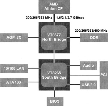
Figure 4.28: Structure of a computer based on the Apollo KT400 chipset
Traditionally, the chipset comprises two components — North Bridge and South Bridge — connected by a special local bus named 8X V-Link (Quad data pump per CLK, 533 MB/sec). The bus is bidirectional, with 266 MB/sec transmitted in any direction of data transfer.
The North Bridge, represented by the VT8377 chip, provides all functions specific for interfacing with the processor, AGP video adapter, main memory, and South Bridge.
The FSB controller built into VT8377 supports bus frequencies of 100/133/166 MHz.
The built-in memory controller ensures support for DDR SDRAM (Double Data Rate SDRAM) and DDR200/266/333, with maximum memory of 4 GB. The maximum data-transmission speed is 1.6/2.1/2.7 GB/sec at DDR200/266/333. Unofficially, this chipset also supports DDR400.
The built-in graphics controller supports one AGP device in 2X/4X/8X modes.
Control over peripheral devices is delegated to the South Bridge, represented by the VT8235 chip. This chip is included in the base set of the Apollo KT400 chipset.
The built-in tools of the base set support the following:
-
Two IDE channels, with support for ATA 33/66/100/133 (up to four IDE devices)
-
Three USB 2.0 controllers (six ports) and five PCI
-
LPC Super I/O (Low Pin Count)
-
AC'97 with support for six audio channels (Surround Sound AC-97 Audio)
-
MC'97, VIA 10/100 Ethernet MAC (Media Access Control), Advanced Communications Riser (ACR), ACPI, advanced power management, and other devices and functions
Popular Motherboards
When evaluating the parameters of contemporary motherboards, it is expedient to consider high-performance motherboards that have the greatest popularity, are produced by well-known companies, and frequently are used in systems that operate in overclocked modes.
Abit BE6-II
Processors: Intel Pentium II/III, Celeron, Slot 1. Chipset: Intel 440BX AGPset. FSB frequencies: 66/75/83-200 MHz incremented at a step equal to 1 MHz. Processor core supply voltage: 1.3–2.3 V with a 0.05 V increment. RAM: Three DIMM, up to 768 MB SDRAM, ECC. Video: AGP 1X/2X. ATA: Two Ultra DMA/33 IDE ports, two Ultra DMA/66/33 (HPT366) ports. I/O: Two serial ports, one parallel port (ECP/EPP), two USB, PS/2, Infrared Data Association (IrDA), floppy. Technologies: ACPI; hardware monitoring; Wake-on-LAN header, Wake-on-Ring header, and waking on from events generated by the keyboard, mouse, network, and modem. BIOS: Award BIOS v.6, Plug-and-Play, Write-Protect Anti-Virus, SoftMenu III (or DIP switches for setting the CPU parameters). Slots: Five PCI, one ISA, one AGP. Form factor: ATX (305 × 200 mm).
Abit KT7
Processors: AMD Athlon/Duron, Socket A. Chipset: VIA Apollo KT133 (VT8363+VT82C686A). FSB frequency: 100 MHz (Alpha EV6). Overclocking: CPU core supply voltage of 1.1–1.85 V with an increment of 0.25 V. FSB frequencies: 100/101/103/105/107/110/112/115/117/120/122/124/127/133/136/140/145/150/155 MHz. RAM: Three DIMM, up to 1.5 GB PC100/PC133 SDRAM, memory-bus frequency of 100/133 MHz. Video: AGP 1X/2X/4X. ATA: Two IDE ports (up to four Ultra DMA/66/33 devices). I/O: Two PS/2 slots for connecting keyboard and mouse, one floppy port, one parallel port (EPP/ECP), two serial ports, two USB ports (with two additional), and so on. BIOS: Award Plug-and-Play. Slots: One AGP, six PCI, one ISA. Form factor: ATX (305 × 230 mm).
There is also an extended version of the Abit KT7 motherboard: Abit KT7-RAID. Architecture of this version employs the HPT370 (Ultra DMA/100, RAID) chip. RAID allows the operating speed to be increased and the reliability of data storage on hard disks to be improved. The presence of the HPT370 chip allows an increase to eight IDE devices.
The Abit KT7 motherboard allows the CPU frequency multipliers to be unlocked. However, this is possible only when L1 bridges on the surface of Athlon or Duron processors weren't cut during fabrication and testing by the manufacturer. If this isn't the case, you should use the technology for restoring these bridges.
After the release of the VIA Apollo KT133A chipset, Abit designed a new variant of its motherboard architecture, known as Abit KT7A. This board, in contrast to its prototype, has a wider range of FSB frequencies at which stable operation can be achieved. In addition to the possibilities of changing the frequency multiplier of the CPU, it provides optimal capabilities for overclocking.
Abit IT7-MAX2
Processor: Intel Pentium 4 and Celeron (Socket 478) with FSB QPB 400/533 MHz. Chipset (for v.2.0): Intel 845PE/ICH4, Ultra DMA 33/66/100 support, AGP slot with support for AGP 4X (only 1.5 V). Memory: Three 184-pin DIMM (unbuffered non-ECC DIMM), support for three DIMM DDR SDRAM 200/266 (maximum 2 GB). Serial ATA: Integrated two-channel Serial ATA interface, 1.5 Gbit/sec. ATA133 RAID: HighPoint Technologies HPT374 IDE RAID controller. Media XP (add-on): Support for Memory Stick, Secure Digital and Type I/II CompactFlash card readers, wireless devices and S/PDIF I/O for microphone/headphones/USB 2.0/ IEEE 1394. Audio: Six-channel AC'97 codec. USB 2.0: Ten USB 2.0 ports. IEEE 1394: Three IEEE 1394 ports. Network controller: Integrated RTL8100B 10/100M PCI Fast Ethernet. BIOS: SoftMenu technology for setting CPU parameters, Plug-and-Play support, ACPI interface support. Internal I/O slots: One AGP slot, four PCI slots, floppy drive for diskettes up to 2.88 MB, two Ultra DMA 33/66/100 slots, two Ultra DMA 33/66/100/133 (RAID) slots, two Serial ATA slots (1.5 Mbit/sec), six-channel FPIO audio splitter (for Media XP), two USB splitters, one IEEE 1394 splitter, two CD-IN sockets, one IrDA socket. Sockets on the rear panel: One PS/2 socket, one socket for PS/2 mouse, four USB connectors, two IEEE 1394 connectors, S/PDIF output, audio sockets (central speaker/subwoofer, speaker for stereo sound), audio sockets (front speakers, linear input, microphone input), two USB sockets, one RJ45 LAN socket. Form factor: ATX. Hardware monitoring: Fan rotation speed, supply voltages, system temperature, Wake Up by LAN, Modem Ring, RTC Alarm, keyboard/mouse power-on, STR (Suspend to RAM).
DDR SDRAM modules can operate in either synchronous or asynchronous mode. To choose and set the required modes of operation for the processor, memory, and I/O devices, use the appropriate options from the BIOS Setup menu.
For overclocking fans, there are options that can be used to set the CPU overclocked modes. This can be done by increasing the FSB frequency and the memory-bus frequency, and by choosing the optimal values for DDR SDRAM parameters. A photo of this motherboard is in Fig. 4.29.
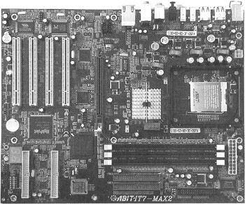
Figure 4.29: Abit IT7-MAX2 Rev. 2.0 motherboard
Asus P3B-F
Processors: Intel Pentium II/III and Celeron, Slot 1.Chipset: Intel 440BX AGPset. FSB frequency: 66/100 MHz. Overclocking: 66/75/83/100/103/105/110/112/115/120/ 124/133/140/150 MHz. Memory: Four DIMM, 8 MB to 1,024 MB, PC100 SDRAM, ECC. Video: AGP 1X/2X. ATA: Two Ultra DMA/33, support for ATAPI IDE CD-ROM and LS-120. I/O: Two serial ports, one parallel port (ECP/EPP), two USB ports, IrDA, two PS/2, floppy (up to 2.88 MB). Technologies: Hardware monitoring, waking from keyboard. BIOS: 2 Mbit Flash Award BIOS v.6.0, ACPI, Plug-and-Play, Anti-boot Virus. Slots (three variants): Six PCI, zero ISA, and one AGP; six PCI, one ISA, and one AGP; or five PCI, zero ISA, and one AGP. Form factor: ATX (192 × 304 mm).
The Asus P3B-F motherboard has become one of the most popular high-performance motherboards.
Asus TUSL2-c
Processors: FC-PGA (PGA2) Intel Pentium III and Celeron, including Tualatin, Socket 370. Chipset: Intel 815EP (82815EP Step B, 82801BA, 82802AB). FSB frequency: 66/100/133 MHz. Overclocking: Capabilities are provided. Memory: Three DIMM, up to 512 MB PC100/PC133 SDRAM. ATA: Two Ultra DMA/33/66/100. I/O: Two serial ports, one parallel port (ECP/EPP), two built-in and two add-on USB ports, two PS/2, floppy. Video: AGP 4X. Audio: CMI8738 audio chip from C-Media. Technologies: Hardware monitoring and wake from modem, mouse, keyboard, and timer. BIOS: 4 Mbit Flash Award BIOS, ACPI, DMI, Green, Plug-and-Play, Trend Chip Away Virus, Symbios SCSI BIOS. Slots: Six PCI, one AGP, one CNR. Form factor: ATX (208 × 305 mm).
Asus P4PE
Processor: Intel Pentium 4 (HT support) and Celeron, Socket 478. Chipset: Intel 82845PE Memory Controller Hub (MCH), 82801DB Enhanced I/O Controller Hub (ICH4). Overclocking: Changing the FSB frequency from 100 MHz to 200 MHz with an increment of 1 MHz, and changing the core supply voltage for CPU, memory, and AGP. Memory: Three 184-pin DIMM DDR SDRAM 200/266/333 (maximum 2 GB). Video: AGP 4X. Audio: AC'97 codec, Analog Devices AD1980. ATA: Two Ultra DMA/33/66/100 and Promise PDC20376, supports Serial ATA (two channels). I/O: Two serial ports, one parallel port (ECP/EPP), two PS/2, floppy, six USB 2.0, two FireWire (VIA6307). Network controller: Broadcom BCM5702CKFB (Gigabit Ethernet). BIOS: 4 Mbit Award BIOS v. 6.0. Slots: Six PCI, one AGP. Form factor: ATX (305 × 230 mm).
Asus P4P800 Deluxe
Processors: Intel Pentium 4 (HT support) and Celeron, Socket 478. Chipset: 865PE Memory Controller Hub (MCH), 82801ER Enhanced I/O Controller Hub (ICH5R). Overclocking: Changing the FSB frequency from 100 MHz to 400 MHz with an increment of 1 MHz, and changing the core supply voltage for the processor, memory, and AGP. Memory: Four DIMM DDR SDRAM, maximum memory of 4 GB, support for one or two memory channels. Video: AGP 4X. Expansion slots: AGP, five PCI. I/O: One FDD, two COM, one LPT, two PS/2, eight USB 2.0, two FireWire, IDE-controller integrated into the chipset (ATA100+SATA RAID), external IDE controller VIA VT6410 (ATA133 RAID). Sound: AC'97 Analog Devices AD1985 codec. Built-in network controller: 3COM Marvell 940-MV00 (Gigabit Ethernet). BIOS: 4 Mbit AMI BIOS v2.51. Form factor: ATX (305 × 245 mm).
A photo of this motherboard is in Fig. 4.30.
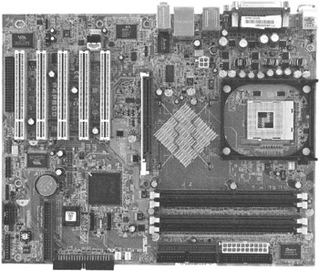
Figure 4.30: Asus P4P800 Deluxe motherboard
Asus P4C800 Deluxe
Processors: Intel Pentium 4 (HT support) and Celeron, Socket 478. Chipset: Intel 875P/ICH5 (RG82875P + FW82801EB). Memory: Four DIMM DDR SDRAM, maximum physical memory of 4 GB, support for one or two memory channels. Video: AGP 4X. Expansion slots: AGP Pro, five PCI. I/O: One FDD, two COM, one LPT, two PS/2, eight USB 2.0, two FireWire, IDE controller integrated into the chipset (ATA100 + SATA), external IDE controller Promise PDC20378 (SATA/ATA133 RAID). Sound: AC'97 Analog Devices AD1985 codec. Built-in network controller: 3COM Marvell 940-MV00 (Gigabit Ethernet). BIOS: 4 Mbit AMI BIOS v2.51. Form Factor: ATX (305×245 mm).
A photo of this motherboard is shown in Fig. 4.31.
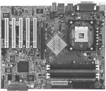
Figure 4.31: Asus P4C800 Deluxe motherboard
Intel D845PEBT2
Processor: Intel Pentium 4 and Celeron processors (Socket 478) with FSB QPB operating at 400/533 MHz, support for hyperthreading technology. Chipset: Intel 82845PE (MCH)/82801DB (ICH4). Memory: Two slots (184-pin) for DIMM (unbuffered Non-ECC DIMM), DDR266/333, maximum memory of 2 GB. Audio: Integrated six-channel AC'97 codec (AC'97 Audio with SoundMAX Cadenza). USB 2.0: Up to six USB 2.0 ports with a data-transmission rate up to 480 Mbit/sec. LAN: Integrated 10/100 Mbit Ethernet network controller. BIOS: 4 MB Flash EEPROM, automatic configuration of IDE devices, Intel Rapid BIOS boot technology to speed up the POST routine. Internal slots: One AGP, six PCI, one floppy port (supports devices up to 2.88 MB), two Ultra DMA 100/66/33 connectors, two USB 2.0. External slots: One PS/2 keyboard, one xPS/2 mouse, four USB 2.0, RJ45-LAN network slot, one parallel port, one COM port, audio sockets (line-in, mic-in, line-out). Hardware monitoring: Voltage and temperature monitoring, automatic control over the fan rotation speed. Form factor: ATX.
The Intel D845PEBT2 motherboard implements the Intel Rapid BIOS boot technology and Burn-In Mode technology for processor overclocking. Clock frequencies can be changed from the nominal as follows: -2%, -1%, +1%, +2%, +3%, and +4%. This mode is intended for professionals experimenting with system operating modes that differ in performance, heat emission, and stability. A photo of this motherboard is in Fig. 4.32.
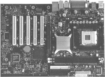
Figure 4.32: Intel D845PEBT2 motherboard
Intel D875PBZ
Intel has designed the D875PBZ motherboard as a dual-channel solution for the main memory subsystem. The architecture of this motherboard, based on the Intel 875P (Canterwood) chipset, implements some promising new technologies. This motherboard is oriented toward high-performance computer systems and ensures support for Intel Pentium 4 processors with hyperthreading technology. It is intended to operate at FSB frequencies of 200 MHz and 133 MHz.
Processor: Intel Pentium 4 processors with hyperthreading technology (bus data rate of 533/800 MHz) in a 478-pin mPGA case. Chipset: Intel 82875P (MCH)/ 82801EB (ICH5R)/82802AC (FWH), two Serial ATA 150 ports with support for Intel RAID 0, Ultra ATA 66/100, five PCI slots, ACPI 1.0b, corresponding to PC2001 specifications. RAM: Four 184-pin slots for DIMM, DDR333/400, 2.5 V, ECC supported, maximum memory of 4 GB, support for one or two memory channels. USB 2.0: Six ports on the rear panel (one doubled and one quadrupled), two ports on the front panel (contact group for outputs on the front panel). Video: AGP 3.0 with support for the AGP 8X mode. Audio: Audio subsystem complying with the Flex 6 standard based on the AD1985 codec from Analog Devices (specific requirement from the customer). LAN: Integrated Gigabit Ethernet network controller (with the CSA interface). BIOS: 8 MB Flash EEPROM with Intel/AMI BIOS, automatic configuration of IDE devices, Intel Rapid BIOS boot technology to speed up the POST routine. Internal slots: One AGP, five PCI, one floppy port (supporting devices up to 2.88 MB), two Ultra DMA 33/66/100 connectors, two Serial ATA 150 connectors, two USB 2.0 connectors. External connectors: PS/2 keyboard and mouse, six USB 2.0 sockets, one RJ45-LAN network socket, one parallel port, one serial (COM) port, audio sockets (line-in, mic-in, line-out). Hardware monitoring: Temperature and voltage monitoring, automatic control over fan rotation speed (Intel Precision Cooling). Form factor: ATX 2.30 (237.5 × 240 mm).
Like Intel D875PBT2B, the Intel D875PBZ motherboard implements new technologies such as Intel Rapid BIOS boot and processor Burn-In Mode. Clock frequencies can be changed from the nominal as follows: -2%, -1%, +1%, +2%, +3%, and +4%. The overclocking mode is intended for professionals experimenting with modes of system operation that differ in performance, heat emission, and stability. A photo of this motherboard is shown in Fig. 4.33.
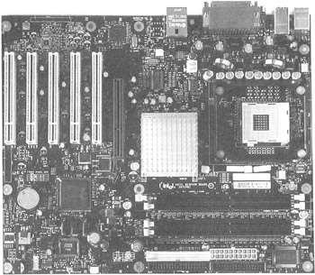
Figure 4.33: Intel D875PBZ motherboard
|
| < Day Day Up > |
|
EAN: 2147483647
Pages: 111