Section 11.5. Moving the Application to Hardware
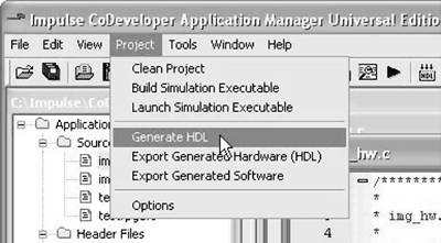
11.5. Moving the Application to HardwareIn this section we will detail the steps required to move the completed application (the image filter and its corresponding embedded test bench process) onto an Altera-based FPGA reference board. The board that we will use is included with the Altera's Nios Development Kit, Stratix Edition, and includes a single Stratix EP1S10 device and a variety of peripherals useful for creating and testing system prototypes. Note The FPGA design software used in this example is Altera's Quartus II, version 4.0 and Altera's SOPC Builder. The specific steps shown may differ in later versions of the Altera tools. The required steps using the Altera software are similar to those described in Chapter 9, in which the triple-DES example was implemented on a Xilinx platform. As with that earlier example, our goal is to create an embedded software test bench operating on the Nios II processor that sends test data (in this case using shared memory) to the FPGA-based image filter. Generating the FPGA HardwareThe first step, after validating the application in desktop simulation, is to compile and generate the HDL and related output files. We'll do this by first selecting a platform target, which will be an Altera FPGA used in conjunction with an embedded Nios II soft processor core. To specify a platform target, we open the Generate Options dialog in the Impulse tools (as shown in Figure 11-14) and specify Altera Nios II. We also specify hw and sw for the hardware and software directories, as shown, and we specify Quartus for the hardware and software export directories. Figure 11-14. Setting hardware generation options for the Altera Nios II target.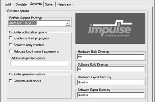 When we select the Generate HDL item from the Impulse tools, as shown in Figure 11-15, a series of processing steps are performed, as described in earlier chapters. These steps include C preprocessing, analysis, optimization, and HDL code generation, as well as the generation of other files that are specific to the Altera design tool flow. When processing is complete, a number of files are created in the hw and sw subdirectories of our project directory. These files include the following:
Figure 11-15. Generating the FPGA hardware.
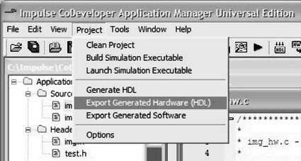
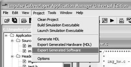
Exporting the Generated FilesAs you saw in the previous step, the Impulse tools create a number of hardware and software-related output files that must all be used to create a complete hardware/software application on the target platform. You can, if you wish, copy these files manually and integrate them into an existing Altera project. You can also export the files into the Altera tools semi-automatically. Recall that we specified the directory Quartus as the export target for hardware and software. These export directories specify where the generated hardware and software processes are to be copied when the Export Software and Export Hardware functions are invoked in the Impulse tools. Within these target directories (in this case we have specified both directories as Quartus), the specific destination for each file is determined from the platform support package architecture library files. It is therefore important that the correct platform support package (in this case Altera Nios II) be selected prior to starting the export process. To export the files from the build directories (in this case hw and sw) to the export directories (in this case the Quartus directory), we select Export Generated Hardware (HDL) and Export Generated Software, as shown in Figure 11-16. Figure 11-16. Exporting the image filter hardware and software.
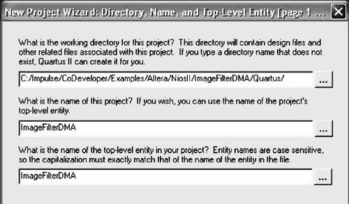
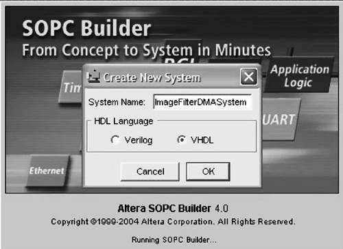
We have now exported all necessary files from the Impulse tools to the Quartus project directory. Note The sections that follow make extensive use of the Altera SOPC Builder software. This software is updated frequently and the steps shown may change substantially in future versions. Creating a New Quartus and SOPC Builder ProjectNow we'll move into the Altera tool environment. We begin by launching Altera Quartus II and opening a new project using the New Project Wizard. In the field prompting us for the new project's working directory, we click the Browse button and find the directory (Quartus) to which we exported the hardware and software files in the previous step. We select the Quartus directory and click Open. On page one of the New Project Wizard dialog, we enter ImageFilterDMA in both the project name and the top-level design entity fields as shown in Figure 11-17. We click Next to move to the next page. Figure 11-17. Creating and naming a Quartus project.
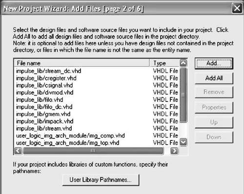
Now we will import the generated VHDL files generated by the tools, as well as create a block diagram file representing the entire system. (Creating the block diagram is not shown here, but it is not difficult using the Altera tools and following the Altera tutorial examples.) We import the files to Quartus in the following order:
The files are listed in Quartus in the opposite order from which they were added. For example, the impulse_lib files appear at the top of the list, as shown in Figure 11-18. Figure 11-18. Adding files to the Quartus project.
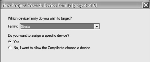
We click Next to proceed and then skip the EDA Tool Settings page (page 3) by again clicking Next. In the Device Family page (page 4), we select the device family we will be targetingin this case Stratix, as shown in Figure 11-19. We click Next, then in the Wizard page that follows we select the specific device we will be targeting. For this example we have chosen EP1S10F780C6ES (see Figure 11-20), which is the device supplied on our prototyping board. Figure 11-19. Selecting the Altera Stratix device.
Figure 11-20. Selecting the target device.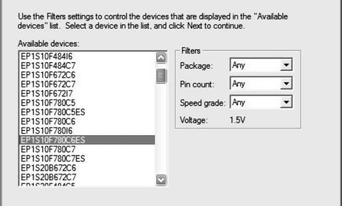 We click Next again to see a summary page listing the options we have chosen. We click Finish to exit the Wizard and return to Quartus. In the next steps we will create and configure a hardware system with a Nios II processor and the necessary I/O interfaces for our sample application. This is a somewhat lengthy procedure but it needs to be done only once, and the resulting platform can be copied and modified for other, similar projects. Creating the New Platform Using SOPC BuilderNow that we have created a Quartus project using the wizard, we need to specify additional information about our platform to support the requirements of the hardware/software application. These steps include the creation of a hardware system with a Nios II processor and the necessary I/O elements. We will use SOPC Builder to create a hardware system containing an Altera Nios II embedded processor, the generated FPGA module representing the ImageFilterDMA hardware process, and several necessary peripherals. To do this, we start SOPC Builder from the Quartus environment, as shown in Figure 11-21. We give the new SOPC Builder project a name (see Figure 11-22) and specify that it is a VHDL project. Figure 11-21. Starting SOPC Builder.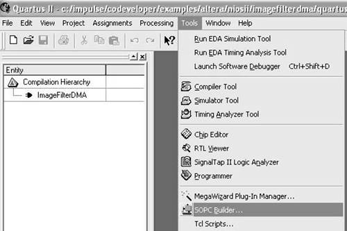 Figure 11-22. Naming the SOPC Builder project.
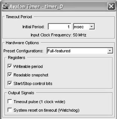
Configuring the FPGA PlatformIn SOPC Builder, we begin by selecting our specific development board in the SOPC Builder dialog, as shown in Figure 11-23. The SOPC Builder software includes a variety of Altera boards as supported targets, including our Stratix-based board. Figure 11-23. Choosing the target board.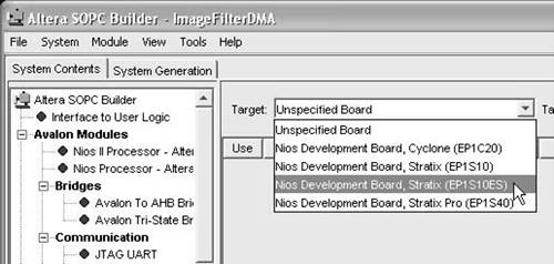 After selecting the board, the next task is to add the largest component of the system, the Nios II processor. From the System Contents tab (on the left side of the SOPC Builder window), we select Nios II Processor - Altera Corporation under Avalon Modules, then click Add. The Altera Nios II configuration Wizard appears. We select the Nios II/s core, as shown in Figure 11-24. We click Finish to add the Nios II CPU to the system and return to SOPC Builder. Figure 11-24. Adding the Nios II processor core.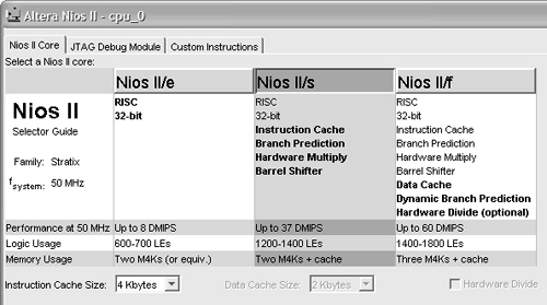 Now we need to rename the Nios II module. We do this by right-clicking cpu_0 in the Module Name column and selecting Rename. We enter the name "cpu" and press the Enter key (see Figure 11-25). Figure 11-25. Naming the CPU.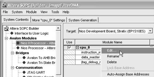 Adding Nios II PeripheralsNext we must add the necessary peripherals to the new Nios II system. Detailed instructions on how to do this are provided in the documentation that comes with the Nios II Development Kit and in tutorials provided by Altera. The following steps summarize what needs to be done for each component in the system. The Timer PeripheralTo add the timer peripheral, system_timer, we perform the following steps:
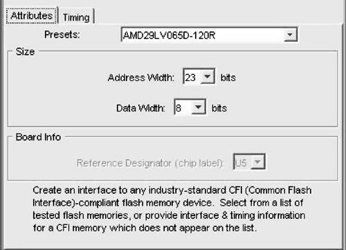
External Flash Memory InterfaceTo add the external Flash peripheral, ext_flash, we perform the following steps:
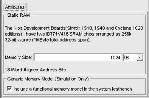
External RAM InterfaceTo add the external RAM peripheral, ext_ram, we perform the following steps:
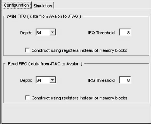
JTAG UART InterfaceThe JTAG UART is used for communication between the board and the host machine and for debugging software running on the Nios II processor. To add the JTAG UART peripheral, jtag_uart, we perform the following steps:
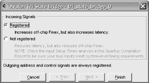
External RAM Bus (Avalon Tri-State Bridge)For the Nios II system to communicate with memory external to the FPGA on the development board, we must add a bridge between the Avalon bus and the bus or buses to which the external memory is connected. To add the Avalon tri-state bridge, ext_ram_bus, we perform the following steps:
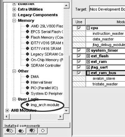
Adding the Hardware Process Module (img_arch)We will now add the img_arch module, which implements the ImageFilterDMA hardware process. To do this, we double-click User Logic under Avalon Modules in the System Contents pane. We then select the img_arch module and click Add (see Figure 11-31). We make sure the name assigned to the img_arch module item is user_logic_img_arch_module_0. Figure 11-31. Adding the image filter logic.
Next, we connect the new img_arch module to the shared Avalon Bus. To do this, we position our mouse pointer over the open circle at the intersection of the user_logic_img_arch_module_0 (avalon) column and the row named avalon_slave under ext_ram_bus, and then click the mouse button (see Figure 11-32). The open circle turns black to indicate a bus connection. Figure 11-32. Connecting the image filter block to the Avalon bus.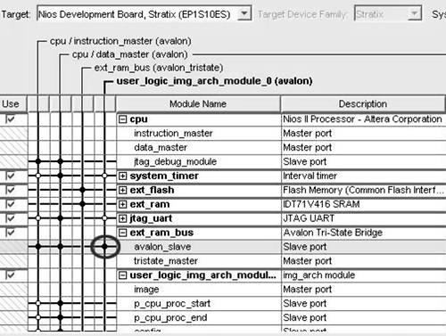 We have now finished adding the necessary peripherals. Setting Additional CPU SettingsA few additional settings can be configured using the More "cpu" Settings dialog in SOPC Builder. For our platform, we will need only to change the Memory Module setting of the Reset Address Processor Function to ext_flash, as shown in Figure 11-33. Once this is done, our new Nios II platform is ready for system generation. Figure 11-33. Changing the Memory Module setting.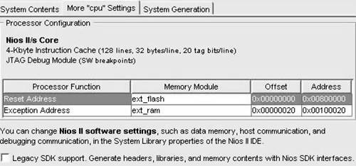 Generating the SystemAt this point we have set up and configured our new Nios II-based platform, including the hardware module generated for the image filter. We can now start the system generation process within SOPC Builder. To do this, we click the System Generation tab in SOPC Builder and make sure the HDL option is selected. We click Generate to generate the system. This process, which takes several minutes, generates a series of log messages similar to those shown in Figure 11-34. When generation is complete, we exit SOPC Builder and return to Quartus. Figure 11-34. Building the SOPC Builder project.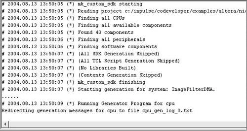 Connecting the Generated System to FPGA PinsNow we need to use the Quartus block diagram editor to connect the complete SOPC Builder-generated system (which includes the ImageFilterDMA hardware process module, the Nios II processor, and peripherals) to the pins on the FPGA. To do this, we open the block diagram file by selecting the Files tab in the project explorer window. We double-click on the entry for file ImageFilterDMA.bdf, which is located in the Device Design Files folder. The block diagram file appears, as shown in Figure 11-35. Figure 11-35. Opening the BDF file.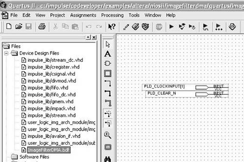 Now we add the block representing the SOPC Builder-generated system. We double-click anywhere in the open block diagram file to bring up the Symbol dialog and then open the Project folder and select the symbol named ImageFilterDMASystem, as shown in Figure 11-36. After we click OK, a symbol outline appears attached to the mouse pointer. We align the outline with the pins on the block diagram and click once to place the symbol, as shown in Figure 11-37. Figure 11-36. Creating a symbol for the image filter block.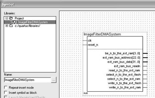 Figure 11-37. Aligning the pins.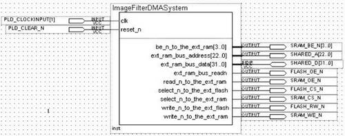 FPGA Pin AssignmentThe next step is to assign pins on the FPGA. Instead of assigning each individual pin (a tedious process), we can use a Tcl script that does the pin assignments for us. To run the Tcl script, we choose Tcl Scripts from the Quartus Tools menu. The dialog of Figure 11-38 appears. We select stratix-pins in the Project folder and click Run to assign the pins in the design. Figure 11-38. Using a script to assigning pins for the image filter block.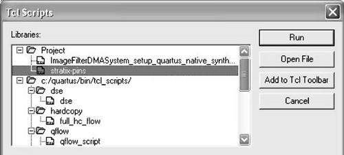 The project is now (finally!) ready for bitmap generation and subsequent downloading. At this point we will probably want to save the project as a template for use with other Impulse C projects. Generating the FPGA BitmapAt this point we have successfully done the following:
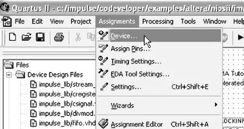
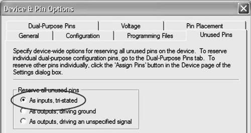
We are now ready to generate the bitmap and download the complete application to the target platform. This process is not complicated (at least in terms of your actions at the keyboard), but it can be time-consuming due to the large amount of processing that is required within the Altera tools. First, we must apply some compiler settings related to pin assignment. We select Assignments -> Device from the Quartus menu to open the Device Settings dialog, as shown in Figure 11-39. We then click the Device & Pin Options button to open the Device & Pin Options dialog, as shown in Figure 11-40. Figure 11-39. Setting device options in Quartus.
Figure 11-40. Setting device and pin options.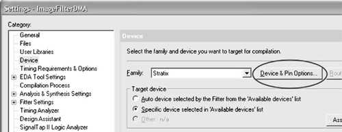 In the dialog that appears, we select the Unused Pins tab, then set the Reserve all unused pins option to As inputs, tri-stated (see Figure 11-41). Figure 11-41. Setting unused pins as inputs.
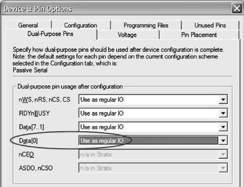
Next, we select the Dual-Purpose Pins tab and specify "Use as regular IO" for all dual-purpose pins listed (Figure 11-42). Figure 11-42. Setting dual-purpose pins.
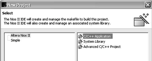
Now we're ready to synthesize, download, and run the application. To generate the bitmap, we select Processing -> Start Compilation, as shown in Figure 11-43. This process requires around 30 minutes to complete on our development system. Figure 11-43. Starting processing in Quartus.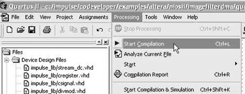 During compilation, Quartus analyzes the generated VHDL source files, synthesizes the necessary logic, and creates logic that is subsequently placed and routed into the FPGA along with the Nios II processor and interface elements that were previously specified. The result is a bitmap file (in the appropriate Altera format) ready for downloading to the device. When the bitstream has been generated, we select Tools > Programmer to open a new programming file. We select File -> Save As and save the chain description file as ImageFilterDMA.cdf, making sure the "Add file to current project" option is selected. The programming file ImageFilterDMA.sof is now visible in the programming window. We enable Program/Configure for the download file named ImageFilterDMA.sof, and make sure our programming hardware (in this case the ByteBlasterMV cable) is configured properly. We click Start (see Figure 11-44) to begin downloading the ImageFilterDMA.sof file to the target device. With the hardware programmed, we are ready to download and run the software application on the Nios II platform. Figure 11-44. Programming the device.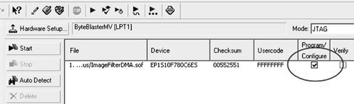 Running the Test Application on the PlatformIn the previous step, we programmed the FPGA device with the design we created in Quartus and SOPC Builder. Now we will use Altera's Nios II IDE (which is based on the popular Eclipse open-source development environment) to compile the software portion of the project and run it on the development board. We begin this process by starting the Nios II IDE. We create a new Nios II project to manage the ImageFilterDMA software files. After we select File -> New -> Project, the wizard shown in Figure 11-45 appears. We select Altera Nios II and C/C++ Application, as shown, and click Next. Figure 11-45. Creating a new software project.
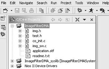
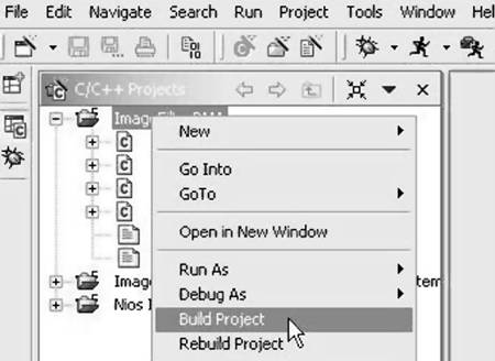
On the next page we select the project path, target hardware, and project template, using the Browse buttons to locate the appropriate Path and SOPC Builder System options, as shown in Figure 11-46. The project path is set to the directory containing the software files that were exported by the Impulse tools. We click Finish to create the new project. Figure 11-46. Creating the new Nios II project.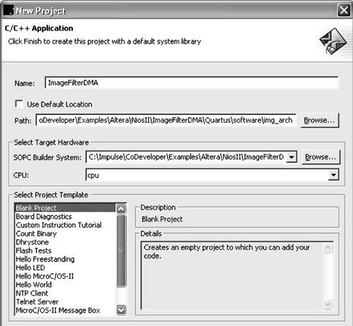 Two new projects (ImageFilterDMA and ImageFilterDMA_syslib) now appear in the C/C++ Projects window in the Nios II IDE, as shown in Figure 11-47. We can now build the project by right-clicking the ImageFilterDMA project and selecting Build Project from the menu that appears (see Figure 11-48). The IDE builds the ImageFilterDMA_syslib system library, which includes a driver for the Impulse C hardware module created by the Impulse tools, along with the application software code in the ImageFilterDMA project. Figure 11-47. Adding software files to the new project.
Figure 11-48. Building the project.
Once the software has finished building, we are ready to run the application in hardware. We right-click the ImageFilterDMA project and select Run As -> Nios II Hardware. We see printed output in the Console window (see Figure 11-49) that lets us verify the output of the hardware against some expected results, which in this test are statically-defined values as shown. Figure 11-49. Nios II console output.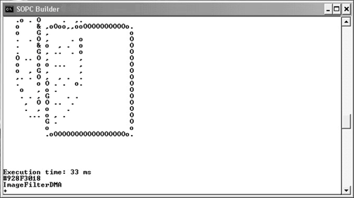
|
EAN: 2147483647
Pages: 208