5.3 Low-Power Design Techniques and Methodologies
Low-power techniques vary depending on the level of the design targeted , ranging from semiconductor technology to the higher levels of abstraction. These abstraction levels are classified as algorithm, architecture, RT, gate, and transistor levels. Figure 5.4 shows various levels of hierarchy that should be considered for low-power designs.
Figure 5.4. Levels of Design Power Optimization
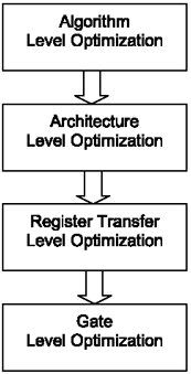
The higher levels of design abstraction shown in Figure 5.4 provide larger amounts of power reduction for chip designs. In higher levels of abstraction, such as algorithm level, designers have a greater degree of freedom to implement low-power design techniques. Hence, power-optimization process is the most effective method in higher levels of abstraction.
As we move toward the lower levels, the amount of power savings becomes less significant and the speed of power optimization becomes slower. Lower level power-optimization techniques are more accurate; however, they are not as fast as higher level methods. Table 5.1 illustrates the amount of power savings for various optimization methods .
It's important to mention that a successful power-optimization methodology requires low-power techniques to be carefully considered at each level of design abstraction.
In previous chapters, we covered the design flow and methodologies for front-end and back-end designs. Figure 5.5 shows a typical low-power design flow. In this figure, the RT-level and gate-level simulation databases and switching-activity data are input to the corresponding power-optimization engines. Here, the last stage in power optimization is performed at transistor level where a low-power library is used.
Figure 5.5. Low-Power Design Flow
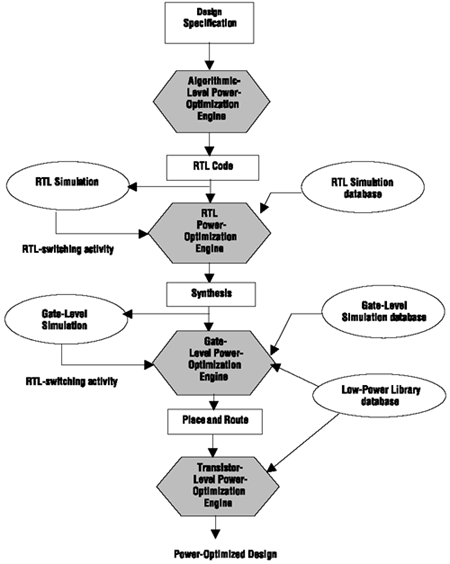
Table 5.1. Power-Saving Percentage per Optimization Method
| Optimization Method | Power-Saving Percentage |
|---|---|
| Algorithm Level | 75% |
| Architecture Level | 50% “75% |
| Register Transfer Level | 15% “50% |
| Gate Level | 5% “15% |
| Transistor Level | 3% “5% |
As mentioned in previous sections, short-circuit and static power dissipations have minimal effect on overall power consumption and can be minimized by selecting the appropriate physical components and process technologies. Therefore, dynamic power is the only source of dissipation that can be effectively managed through proper design techniques. In order to optimize power in a design successfully, dynamic power in each individual component (memories, interconnects, processors, cores, etc.) has to be estimated and minimized separately. Reducing the dynamic power requires the minimization of all parameters in Equation 5.5.
Table 5.2 is a brief summary of various factors involved in saving dynamic power.
The following sections cover several low-power techniques based on reduction of parameters in Table 5.2 at various levels of design abstraction. As mentioned earlier, higher levels of design abstraction contribute more to power savings than do the lower levels. However, power-reduction techniques have to be considered at all levels of design to obtain the best results.
Table 5.2. Factors in Reducing Dynamic Power
| Reduction Parameter | Result |
|---|---|
|
| Saves power by optimizing the excessive transitions through clock gating |
| C | Saves power by using an appropriate process technology or improving the layout |
| V DD | Saves power dramatically but slows down the circuit |
| F | Saves power through reducing the clock frequency but results in slowing down the functionality |
Algorithm-Level Optimization
Algorithm-level optimization provides the highest level of power savings in a design. In this stage, hardware/software partitioning provides power reduction by dividing the tasks between hardware and software. Using HW/SW partitioning, heavy calculations can be performed in the hardware, while control functions can be handled in software. This partitioning reduces the chip's power consumption and minimizes the processor load and bus traffic. An example of HW/SW partitioning is shown in Figure 5.6 in a Voice over Network (VoN) application.
Figure 5.6. HW/SW Partitioning in a VoN SOC
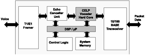
The heart of this SOC is a code excited linear predictive (CELP) core for voice compression/ decompression . The CELP functions in this example are divided between hardware and software. Computationally intensive functions of CELP, such as codebook search and vector quantization, are performed in the hardware, while the system processor is used only for data formatting and control.
Algorithm-level optimization is commonly used in processor and DSP modules/cores. DSP algorithms are computationally intensive. Therefore, reducing the number of operations to execute a given DSP function lowers the switching activity and results in reduced power. Most DSP algorithms involve several multiplication operations. Multiplication, which is the most power consuming operation in such algorithms, can be replaced by shift-add operations to reduce power. For example, this method can be useful in finite impulse response (FIR) filter designs. Figure 5.7 represents an FIR filter implementation diagram.
Figure 5.7. General FIR-Filter Implementations
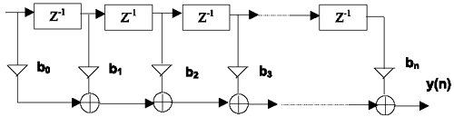
As shown in Figure 5.7, in an FIR filter an array of constant tap coefficients is multiplied by an array of delayed data samples. The resulting array is summed with the most recent data samples after each multiplication. Multiplication by constant coefficients can be replaced by shift-add operations to lower the power consumption in such filters.
Architecture-Level Optimization
According to Equation 5.5, power is dependent on the supply voltage squared. Therefore, minimizing the supply voltage will result in remarkable savings in power consumption. One approach for power optimization using supply-voltage reduction is to use a common low-supply voltage for all of the logic modules. However, lowering the supply voltage increases the latency in various blocks and as a result decreases the overall speed of the design.
Utilizing multiple supply voltages is another approach to overcoming the problem of large delays that result in lowering the speed of a device. Using this method, each logic block, or each group of logic blocks, can use a unique supply voltage. Applying multiple supply voltages in a chip allows the modules on critical or high-speed paths to meet their timing requirements by using a high supply voltage, whereas the modules on noncritical or low-speed paths can use lower supply voltages. Hence, the power is saved without influencing the overall speed of the design.
The basic idea of minimizing the switching activity to reduce power can also be performed at the architectural level for processors by carefully using arithmetic representations. Two's complement is the most common representation used in DSP blocks/modules. This is because arithmetic operations such as additions and subtractions are easily performed with two's complement. However, the problem with this representation is that its sign extension causes the sign of the most significant bit (MSB) to toggle when signals change sign. To handle this problem, the use of sign-magnitude arithmetic-number representation is recommended. This approach can reduce the switching activity compared to two's complement numbering for negative values. The reason is that in two's complement numbering a large number of unnecessary ones is needed to represent a small negative number. Therefore, the number of bit transitions between positive and negative numbers is large and results in high-transition activity for input signals around zero. The following is an example of two's complement representation from “4 to +4.
| Decimal | Two's Complement |
|---|---|
| “4 | 1100 |
| “3 | 1101 |
| “2 | 1110 |
| “1 | 1111 |
|
| 0000 |
| 1 | 0001 |
| 2 | 0010 |
| 3 | 0011 |
| 4 | 0100 |
As shown in the above example, there is high activity in the shaded area around zero.
Another area where power can be minimized at architectural level is memory. We will cover memory- related power optimizations in later sections.
RT-Level Optimization
RTL power optimization reduces the high activity of signals through clock gating, finite-state-machine (FSM) encoding, bus encoding, and avoiding glitches. Each of these concepts will be covered in detail in the following subsections.
Clock Gating Optimization
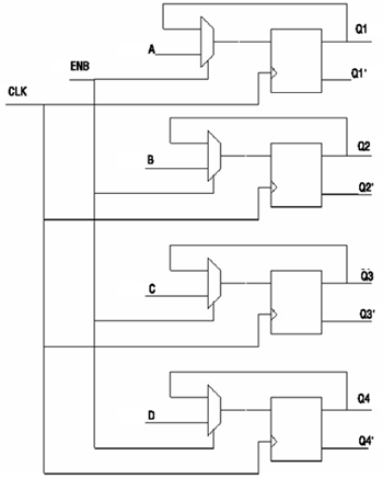
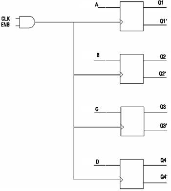
Clock signals in ICs are considered to be the major contributors to power dissipation because they switch at all times. Clocks can be gated to reduce excessive switching in synchronous registers. Figure 5.8 represents a 4-bit register with and without clock gating.
As shown in Figure 5.8b, the clock signal is transitioning continuously at the clock input of all four flip flops. However, when the clock signal is gated, it transitions only at input of the AND gate. As a result, the register with the gated-clock scheme dissipates less power than the one without clock gating. Using this method, the amount of power savings increases as the number of bits in a register increases. Gate-level power-optimization EDA tools automatically add gates to clocks in order to save power. Appendix A provides detailed information on some of the popular EDA power-optimization tools.
Figure 5.8(b). Internal Circuitry of a 4-Bit Register without Gated Clocks
Signal-Encoding Optimization
Power can be reduced in algorithm level by choosing the appropriate coding style. The use of gray codes results in a significant decrease in switching activity. Minimizing the number of transitions in the state assignment of an FSM has a considerable influence on lowering the power consumption. If the next state of an FSM differs by one variable from the preceding state (minimum Hamming distance) activities are minimized and power can be saved considerably. Therefore, gray coding is preferred to binary coding in state assignment of FSMs. Table 5.3 illustrates binary coding and gray-coding schemes.
Figure 5.8(a). 4-Bit Synchronous Register
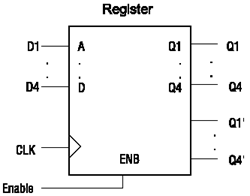
Figure 5.8(c). Internal Circuitry of a 4-Bit Register with Gated Clocks
As shown in Table 5.3, a gray-coding representation of numbers requires fewer transitions than does a binary-coding representation. For example, moving from 3 to 4 in decimal numbers requires three transitions in binary-code representation, while it needs only one transition in gray-code representation. Therefore, less power is consumed when states of an FSM use gray coding.
This technique is also very useful for power reduction in SOC bus interconnects. Buses are significant sources of power dissipation (almost 20 percent of total power dissipation in most SOCs are due to bus interconnects) because of their high switching activity and large capacitive loading. Therefore, bus signal encoding is very effective in lowering the switching activity. Equation 5.6 shows how Equation 5.5 can be modified to represent power dissipation in bus interconnects.
Table 5.3. Transition Activity of Binary Coding versus Gray Coding
| Decimal | Binary Code | Number of Transitions | Gray Code | Number of Transitions |
|---|---|---|---|---|
|
| 000 |
| 000 |
|
| 1 | 001 | 1 | 001 | 1 |
| 2 | 010 | 2 | 011 | 1 |
| 3 | 011 | 1 | 010 | 1 |
| 4 | 100 | 3 | 110 | 1 |
| 5 | 101 | 1 | 111 | 1 |
| 6 | 110 | 2 | 101 | 1 |
| 7 | 111 | 1 | 100 | 1 |
Equation 5.6
![]()
where n is the number of bits in a bus.
Since dynamic power is directly related to bus width, bus segmentation can provide considerable power reduction in interconnects by reducing capacitance in each bus segment.
As mentioned earlier, gray coding can provide less transition activity for bus interconnects. Another commonly used encoding technique is bus invert (BI) coding. In this method, a control signal determines if the actual data or its complement provides fewer transitions to be sent at each clock cycle on a bus interconnect. This decision is made based on the Hamming distance between the present and next state of the data bus. If the Hamming distance is larger than half the bus width (n/2), the next bus value will be equal to the complement of the next data value. If the Hamming distance is smaller than n/2, the bus value will be equal to actual data value.
Partial bus invert (PBI) coding can also be used to reduce the switching activity in interconnects. In this method, a wide bus is segmented to a smaller subset of buses, and the high activity subsets are encoded using bus inverting. All of the mentioned bus encoding techniques reduce the activity in interconnects. However, gray coding is commonly used for instruction buses, BI is used for data buses, and PBI is most common in address buses.
Combinatorial Transitions Optimization (Deglitching)
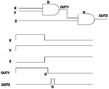
As mentioned earlier, switching activity in CMOS devices is a major cause of power dissipation. Therefore, protecting circuits from unnecessary switching can save power significantly. Glitches are momentary transitions that occur in combinatorial circuits due to delay imbalances in different gates. Figure 5.9 illustrates an example of glitching in a logic block.
Figure 5.9. Glitching in Logic Gates
Since glitches add to the number of signal transitions, they should be avoided whenever possible. As explained in algorithmic level optimization, algorithms that require many multiply-and-add operations, such as filters in general, are prone to produce glitches and consume a lot of power. These arithmetic operations can produce glitches if all of the multipliers and adders are sequential without any latches to hold their value until they become stable. Figure 5.10 represents two different implementations of the multiply-add operation for such algorithms.
Figure 5.10. Implementation of a Multiplier and Adder Tree (a) Non-Latch-Based Implementation
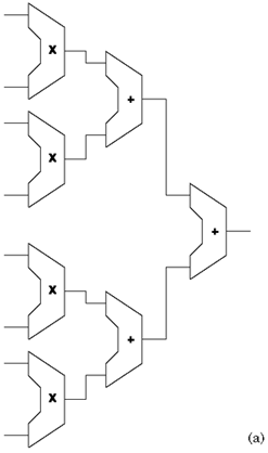
In Figure 5.10a, depending on the delay of adders, the result of each add operation may have glitches until the final stable result occurs. Glitches can propagate to the next level of adders as inputs and then generate momentary wrong results, causing more transitions until the final result is generated. These momentary transitions increase power consumption in the circuit and should be avoided by using latches at the output of each adder and multiplier, as shown in Figure 5.10b.
Figure 5.10. Implementation of a Multiplier and Adder Tree (b) Latch-Based Implementation
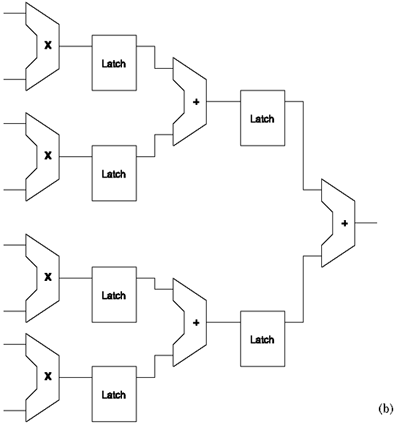
Similar to flip flops, latches save the previous value of the inputs at each level and prevent the extra switching activity that results in glitches and momentary wrong results.
Another low-power design technique that is very common among chip designers is to replace the flip flops with latches whenever possible. Both latches and flip flops are building blocks of sequential circuits and their outputs depend on the current inputs as well as previous inputs and outputs. Figures 5.11 and 5.12 illustrate the difference between a D-latch and a D-flip flop respectively.
Figure 5.11. Positive-Level Triggered D-Latch (a) Logic Symbol (b) Truth Table (c) Timing Diagram
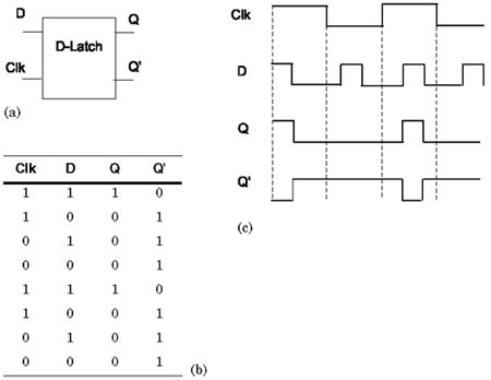
Figure 5.12. Positive-Edge Triggered D-Flip Flop (a) Logic Symbol (b) Truth Table (c) Timing Diagram
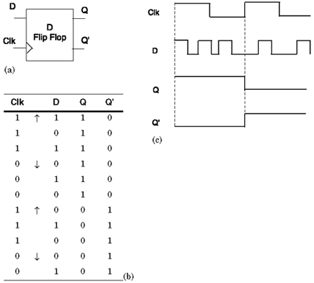
As shown in Figures 5.11 and 5.12, the main difference between latches and flip flops is that latches are level sensitive to clock signal, while flip flops are edge sensitive. For example, in a D-latch, output Q obtains the value of input D for as long as the clock signal is asserted; thus any changes in input will be transferred to output as long as the clock signal is at a specific level (called transparent latch). However, in a D-flip flop, the output changes only at the edge of the clock signal. Therefore, in flip flops the input is transmitted to output only at a specific edge of the clock, while in latches the input is transmitted to output anytime the clock signal is at a specific level. After the rising or falling edge of the clock, the D-flip flop's output remains constant even if input changes.
Memory Optimization
Memories are considered a large factor (about 40 percent) of the total power dissipation in ASICs/SOCs. There are three types of power consumption in memory modules/cores:
-
Power dissipation associated with program and data memory accesses
-
Power required to transmit data across the large capacitance of system interconnects
-
Power consumption within memory units
Memory accesses are power hungry because writing to and reading from memory locations requires high-switching activity on data and address buses. Therefore, in many DSP algorithms, such as image and voice processing, lowering the number of memory accesses required to complete a given function reduces the power consumption in such cores. By having more code in the cache, a designer can minimize the number of power-intensive external accesses to the main memory.
Memory can also be as a group of independent memory sections that can have their own individual clock signals. In this type of architecture, when each memory section is idle, its clock can stop transitioning and the memory segment can be put to sleep mode. Therefore, a large amount of power can be saved when various sections of memory are idle.
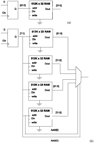
Another popular low-power practice among designers is to split large memories into smaller memory modules. For example, a 512K x 32 RAM can be split into four 128K x 32 RAMs and still provide the same total number of read cycles with lower power dissipation in smaller memories compared to the single large memory. Figure 5.13 illustrates the memory-partitioning approach.
Figure 5.13. (a) Single Large Memory (b) Memory Partitioning
Power Management
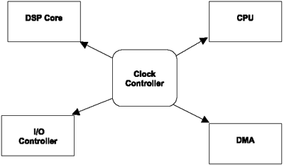
Power management is a technique that controls the power of a chip at various instances by switching off a core (sleep mode) when not needed. It can be done either in software or pure hardware. In a chip with multiple clock domains, various clocks can be gated and a control signal can be used to activate a specific clock only when the block is active. A clock-control block implemented in software or hardware can provide different clock rates to manage various clock domains. To distribute the clock and control the clock skew, a clock tree needs to be constructed using clock buffers. In this approach, some portions of the chip can be shut down at various instances. Figure 5.14 is an example of a clock-control block that delivers separate clock signals to various soft and hard blocks.
Figure 5.14. Clock-Control Block in an ASIC/SOC
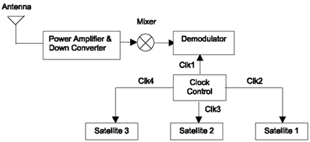
In this technique, different clocks are derived from a master or central clock and can be slowed or stopped under certain conditions to avoid the unused switching activity. Therefore, the load on the master clock is reduced and the flip flops receiving the derived clocks are not triggered when they are on idle cycles. For example, in designing a global positioning system (GPS), several sets of filters per satellite can be controlled by separate clocks. This approach can significantly reduce power consumption in the design of such systems. Figure 5.15 is an example of multiple clock domains in a GPS.
Figure 5.15. Multiple Clock Domains in a GPS
Although gated clocks reduce excessive switching activity and hence the power consumption in synchronous circuits, they can create complexity in static timing verification of such designs. This is because of additional setup time constraint caused by the control signal. EDA STA tools, such as PrimeTime from Synopsys, have shown success in dealing with complex designs having multiple clock domains. It is important to note that clocks are not the only signals that can be gated to save power. Generally, signals with high frequency, such as address or data buses, are also good candidates for signal gating. Power saving becomes more significant when a group of signals share a control signal that has a lower frequency than the source signals.
Gate-Level Optimization
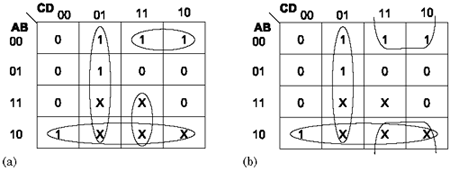
In order to minimize power in the gate level, load capacitances should be minimized by using less logic. Low-power EDA tools usually handle this as part of their optimization techniques. Let's look at a simple example to understand this concept. Here, gate minimization is achieved using proper Boolean functions, followed by appropriate use of don't cares in Karnaugh maps (K-maps).
As shown in Figure 5.16, the use of don't cares in a K-map can make a considerable change in gate count of a logic design. If don't cares are not used properly (as shown in Figure 5.16a), the number of gates used in a design can become very large, resulting in larger silicon area and higher power consumption in designs. Figure 5.16b shows a more careful use of don't cares in K-maps, which illustrates a smaller number of logic gates resulting in less area and less power dissipation for the same design. Once the number of gates is minimized in a design, a low-power library has to be considered for various gates. Reduction of gate power is a relatively simple case of selecting particular libraries with the lowest power characteristics from among various choices of libraries provided by ASIC vendors .
Figure 5.16. Use of K-Maps in Minimizing Logic Gates in a Design (a) Out = AB'+ C'D + A'B'C + ACD + AB'C (b) Out = AB' + C'D + B'C
Proper use of Boolean functions can also save power without reducing the number of logic gates. The following example illustrates the case of power saving without reducing the number of gates at logic level.
Consider the four inputs A, B, C, and D in Figure 5.17. Assuming input A has the highest activity compared to others, we can determine which of the following Boolean functions represents a lower power implementation (if all gates dissipate the same amount of power per signal transition).
-
Out = AB + AC + CD
-
Out = A (B + C) + CD
-
Out = AB + C (A+ D)
Figure 5.17. Logic Required for Three Implementations of a Digital Circuit (a) Out = AB + AC + CD (b) Out = A (B + C) + CD (c) Out = AB + C (A+ D)
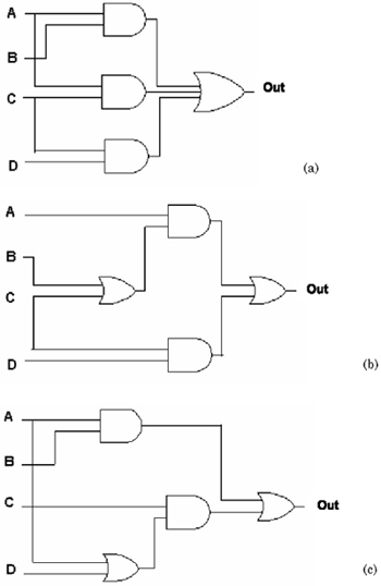
Figure 5.17 provides the logic gates required to build each of the above implementations.
As shown in Figure 5.17, all three implementations require four logic gates. However, the number of logic gates that signal A (i.e., the signal with the highest activity) propagates through represents the amount of power dissipation by each implementation. Signal A in Figure 5.17a propagates through three logic gates. In Figure 5.17b, signal A propagates through two gates and, finally, in Figure 5.17c, it passes through four logic gates. Therefore, the second implementation, Out = A (B + C) + CD , is the most efficient one for low power.
Another gate-level optimization approach is to reduce the transistor sizes. This results in decreasing input capacitances that could as well be the load capacitances for other gates. Although reducing the transistor sizes reduces the capacitance, it also reduces the current derive of each transistor and makes circuits operate slower. For that reason, transistor resizing is an appropriate technique only for noncritical paths in a design.
Power Estimation
To optimize power properly, circuit designers should be able to predict the power at early stages of their design. Power estimation can provide a design criterion for designers by evaluating various design options and the related power efficiencies before they commit to a specific low-power design methodology. Therefore, estimating the power consumption and analyzing the effect of various modifications at different levels of design abstraction are crucial to a successful low-power design.
In order to estimate dynamic power in circuits, the switching activity of different nodes, b , from Equation 5.5 must be calculated. One of the common power-estimation techniques is simulation-based power estimation. In this technique, the circuit under test will be simulated with a set of input stimuli and its power consumption will be monitored continuously. The average power consumed using various input patterns provides an estimation for the power consumption of the device. This method can estimate power in a variety of design styles; however, it is highly dependent on the pattern of input stimuli. This complexity of this technique increases with the number of input stimuli and size of the circuit. Simulation-based power estimation requires that all the input signals provide accurate results. The drawback is that individual blocks cannot be simulated without completing the rest of the design. This is a slow process, and providing all possible combinations of input stimuli for various node activities to estimate power accurately is a challenging task for low-power designers.
Power estimation followed by power optimization can be accomplished with special EDA tools that estimate and minimize the power dissipation at various levels of design abstraction. A more detailed discussion of low-power design tools is provided in the next section.
| |
| Top |
EAN: 2147483647
Pages: 61