4.2 Overview of Physical Design Flow
We reviewed front-end design process in Chapter 1. Figure 4.1 shows a simplified front-end design flow. Here we included floorplanning as part of the front-end design flow. However, many consider floorplanning as a step in the back-end design flow. Whether it is part of front-end or back-end design flow, the main purpose of the floorplanning is to provide the location of blocks, I/Os, and power pads, as well as to define clock and power distributions. In order to do floorplanning, you need to know the gate size and operating frequency of each block in your design.
Figure 4.1. Front-End Design Flow ( Printed with permission of Fujitsu Microelectronics America, Inc.)
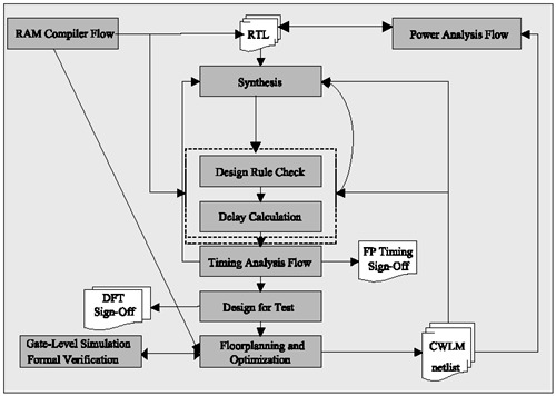
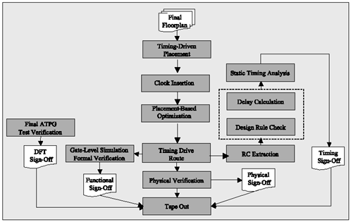
Figure 4.2 shows a simplified back-end design flow. Here, we start with a final floorplan which predicts the size of the chip; then we proceed with timing-driven placement. Timing-driven placement allows for timing optimization based on SDF.
Figure 4.2. Back-End Design Flow (Printed with permission of Fujitsu Microelectronics America, Inc.)
Before planning for your clock insertion, you should know the answers for the following questions:
-
How are the ( core , reference, source, and recovered) clocks distributed?
-
What are the core-clock and recovered-clock frequencies?
-
What is the reference-clock frequency?
-
What is the reference-clock jitter requirement? How is the reference-clock buffering?
-
What are the receiving and sending source-clock frequencies?
-
What is the jitter required for sending clock?
-
What is the jitter on distributed clock?
Clock distribution is one of the most critical aspects of chip design. Criteria for clock distribution are skew and insertion delay, and keeping two values as low as possible. There are several ways to implement clock distribution.
Clock-tree synthesis is a method of implementing clock distribution that generally achieves small skew with relatively low cost (short implementation time with no special cells ). However, it requires aid from CAD tools because the location of distributed clock buffers is critical for skew control. The drawback of this method is that clock insertion delay increases in large chips.
Mesh-based clocking is another scheme which has the following benefits:
-
It is easy to implement, though it requires a unique clock-buffer macro.
-
It is easy to control skew.
-
It does not require any netlist modification to the logic netlist after placement and routing.
However, the disadvantages of this method are required resources for generating clock macros, large power and metal consumptions.
EDA tools are used to generate balanced clock tree. Cadence CTgen is an example of a clock-tree tool.
The goal of the place-and-route stage is to produce a GDSII file for tapeout and also meet timing constraints. The input to place-and-route is I/O specification, gate-level netlist, timing information for critical paths, and clock description. Basically, there are three main steps in routing:
-
Global routing
-
Detailed routing
-
Fixing violations
Global routing provides a plan for reducing the critical path delays as well as the length of interconnects throughout the design. This information plus a congestion map (to show placement routability) are made available for the detailed routing stage to route every net. However, the routing of special nets such as clock and power nets is usually performed before detailed routing.
Detailed routing completes the connections between logic cells and reduces the total logic area and critical path delays throughout the design based on the routing information from global router. The major goal of this stage is to accomplish all of the required interconnects. Channel routing and area-based routing are examples of of detailed routing.
Placement, global routing, detailed routing, and fixing routing violations such as shorts and spacing violations, delay calculation, and clock-tree synthesis are the major tasks performed by place-and-route tools. One popular EDA routing tool is NanoRoute from Cadence Design Systems. NanoRoute performs global and detailed routing, as well as post-routing optimization for any cell-based, block-based , or mixed cell - and block-based designs to reduce the chip-level integration effort. It also fixes the design violations with post-routing optimization to improve the TAT.
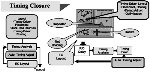
Timing optimization can be divided into two parts : pre-route prediction and post-route correction. Examples of optimization techniques are gate sizing, buffer insertion/deletion, and placement optimization. Figure 4.3 illustrates some of these techniques. PhysicalStudio from Sequence Design, Inc., is an example of a timing-optimization tool.
Figure 4.3. Timing Optimization ( Printed with permission of Fujitsu Microelectronics America, Inc.)
In general, Signal Integrity (SI) issues consist of power problems (voltage drop and electromigration) and timing (crosstalk) problems. Voltage drop or IR drop refers to the drop in the supply voltage across the power distribution network. This affects storage capabilities of RAMs, flip flops, and other storage elements as well as performance and timing failure.
Metal electromigration is a problem that occurs on power wires caused by increased wire resistance and stronger electric fields on finer geometries. These can produce short circuit on adjacent metal lines and broken lines. Electromigration problems worsen with increased current densities and higher temperatures .
Crosstalk problems are caused when the cross-coupling capacitance between two adjacent nets adversely affects the signal integrity of one of the nets. This can result in serious timing problems. Cadence Silicon Ensemble is an example of an EDA tool for crosstalk analysis that you run after routing.
All signal integrity issues have to be resolved for a successful tapeout.
Physical verification consists of the following steps:
-
Design Rule Check (DRC) is necessary to guarantee that a circuit can be fabricated with an acceptable yield. Design rules ensure that the design will not fail due to shorts or process faults.
-
Layout versus Schematic (LVS) compares electrical circuits (source and layout) from the specified sources.
-
Antenna Check ensures that induced capacitance is under a certain value so that electrical characteristics stay stable.
-
Electrical Rule Check (ERC) operations perform tasks related to electrical rule checking that have to be followed by circuit designers. ASIC vendors provide these rules. Examples of ERC violation are open input, short circuit, NMOS connected to Vdd, and PMOS connected to Gnd.
Two popular EDA tools for physical verification are Mentor Calibre and Cadence Dracula.
In order to have a successful tape out, the following sign-off procedures must be complete:
-
Functional sign-off
-
Timing sign-off
-
DFT sign-off
-
Physical sign-off
| |
| |
| Top |
EAN: 2147483647
Pages: 61