[Page 222]3.1. Principles of I/O Hardware Different people look at I/O hardware in different ways. Electrical engineers look at it in terms of chips, wires, power supplies, motors, and all the other physical components that make up the hardware. Programmers look at the interface presented to the softwarethe commands the hardware accepts, the functions it carries out, and the errors that can be reported back. In this book we are concerned with programming I/O devices, not designing, building, or maintaining them, so our interest will be restricted to how the hardware is programmed, not how it works inside. Nevertheless, the programming of many I/O devices is often intimately connected with their internal operation. In the next three subsections we will provide a little general background on I/O hardware as it relates to programming. 3.1.1. I/O Devices I/O devices can be roughly divided into two categories: block devices and character devices. A block device is one that stores information in fixed-size blocks, each one with its own address. Common block sizes range from 512 bytes to 32,768 bytes. The essential property of a block device is that it is possible to read or write each block independently of all the other ones. Disks are the most common block devices. If you look closely, the boundary between devices that are block addressable and those that are not is not well defined. Everyone agrees that a disk is a block addressable device because no matter where the arm currently is, it is always possible to seek to another cylinder and then wait for the required block to rotate under the head. Now consider a tape drive used for making disk backups. Tapes contain a sequence of blocks. If the tape drive is given a command to read block N, it can always rewind the tape and go forward until it comes to block N. This operation is analogous to a disk doing a seek, except that it takes much longer. Also, it may or may not be possible to rewrite one block in the middle of a tape. Even if it were possible to use tapes as random access block devices, that is stretching the point somewhat: they are not normally used that way. The other type of I/O device is the character device. A character device delivers or accepts a stream of characters, without regard to any block structure. It is not addressable and does not have any seek operation. Printers, network interfaces, mice (for pointing), rats (for psychology lab experiments), and most other devices that are not disk-like can be seen as character devices. This classification scheme is not perfect. Some devices just do not fit in. Clocks, for example, are not block addressable. Nor do they generate or accept character streams. All they do is cause interrupts at well-defined intervals. Still, the model of block and character devices is general enough that it can be used as a basis for making some of the operating system software dealing with I/O device independent. The file system, for example, deals only with abstract block devices and leaves the device-dependent part to lower-level software called device drivers.
[Page 223] I/O devices cover a huge range in speeds, which puts considerable pressure on the software to perform well over many orders of magnitude in data rates. Fig. 3-1 shows the data rates of some common devices. Most of these devices tend to get faster as time goes on. Figure 3-1. Some typical device, network, and bus data rates.Device | Data rate |
|---|
Keyboard | 10 bytes/sec | Mouse | 100 bytes/sec | 56K modem | 7 KB/sec | Scanner | 400 KB/sec | Digital camcorder | 4 MB/sec | 52x CD-ROM | 8 MB/sec | FireWire (IEEE 1394) | 50 MB/sec | USB 2.0 | 60 MB/sec | XGA Monitor | 60 MB/sec | SONET OC-12 network | 78 MB/sec | Gigabit Ethernet | 125 MB/sec | Serial ATA disk | 200 MB/sec | SCSI Ultrawide 4 disk | 320 MB/sec | PCI bus | 528 MB/sec |
3.1.2. Device Controllers I/O units typically consist of a mechanical component and an electronic component. It is often possible to separate the two portions to provide a more modular and general design. The electronic component is called the device controller or adapter. On personal computers, it often takes the form of a printed circuit card that can be inserted into an expansion slot. The mechanical component is the device itself. This arrangement is shown in Fig. 3-2 Figure 3-2. A model for connecting the CPU, memory, controllers, and I/O devices. (This item is displayed on page 224 in the print version) 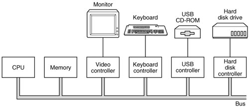
The controller card usually has a connector on it, into which a cable leading to the device itself can be plugged. Many controllers can handle two, four, or even eight identical devices. If the interface between the controller and device is a standard interface, either an official ANSI, IEEE, or ISO standard or a de facto one, then companies can make controllers or devices that fit that interface. Many companies, for example, make disk drives that match the IDE (Integrated Drive Electronics) and SCSI (Small Computer System Interface) interfaces.
[Page 224]We mention this distinction between controller and device because the operating system nearly always deals with the controller, not the device. Most personal computers and servers use the bus model of Fig. 3-2 for communication between the CPU and the controllers. Large mainframes often use a different model, with specialized I/O computers called I/O channels taking some of the load off the main CPU. The interface between the controller and the device is often low-level. A disk, for example, might be formatted with 1024 sectors of 512 bytes per track. What actually comes off the drive, however, is a serial bit stream, starting with a preamble, then the 4096 bits in a sector, and finally a checksum, also called an Error-Correcting Code (ECC). The preamble is written when the disk is formatted and contains the cylinder and sector number, the sector size, and similar data. The controller's job is to convert the serial bit stream into a block of bytes and perform any error correction necessary. The block of bytes is typically first assembled, bit by bit, in a buffer inside the controller. After its checksum has been verified and the block declared to be free of errors, it can then be copied to main memory. The controller for a monitor also works as a bit serial device at an equally low level. It reads bytes containing the characters to be displayed from memory and generates the signals used to modulate the CRT beam. The controller also generates the signals for making a CRT beam do a horizontal retrace after it has finished a scan line, as well as the signals for making it do a vertical retrace after the entire screen has been scanned. On an LCD screen these signals select individual pixels and control their brightness, simulating the effect of the electron beam in a CRT. If it were not for the video controller, the operating system programmer would have to program the scanning explicitly. With the controller, the operating system initializes the controller with a few parameters, such as the number of characters or pixels per line and number of lines per screen, and lets the controller take care of actually driving the display.
[Page 225] Controllers for some devices, especially disks, are becoming extremely sophisticated. For example, modern disk controllers often have many megabytes of memory inside the controller. As a result, when a read is being processed, as soon as the arm gets to the correct cylinder, the controller begins reading and storing data, even if it has not yet reached the sector it needs. This cached data may come in handy for satisfying subsequent requests. Furthermore, even after the requested data has been obtained, the controller may continue to cache data from subsequent sectors, since they are likely to be needed later. In this manner, many disk reads can be handled without any disk activity at all. 3.1.3. Memory-Mapped I/O Each controller has a few registers that are used for communicating with the CPU. By writing into these registers, the operating system can command the device to deliver data, accept data, switch itself on or off, or otherwise perform some action. By reading from these registers, the operating system can learn what the device's state is, whether it is prepared to accept a new command, and so on. In addition to the control registers, many devices have a data buffer that the operating system can read and write. For example, a common way for computers to display pixels on the screen is to have a video RAM, which is basically just a data buffer, available for programs or the operating system to write into. The issue thus arises of how the CPU communicates with the control registers and the device data buffers. Two alternatives exist. In the first approach, each control register is assigned an I/O port number, an 8- or 16-bit integer. Using a special I/O instruction such as IN REG,PORT
the CPU can read in control register PORT and store the result in CPU register REG. Similarly, using OUT PORT,REG
the CPU can write the contents of REG to a control register. Most early computers, including nearly all mainframes, such as the IBM 360 and all of its successors, worked this way. In this scheme, the address spaces for memory and I/O are different, as shown in Fig. 3-3(a). Figure 3-3. (a) Separate I/O and memory space. (b) Memory-mapped I/O. (c) Hybrid. (This item is displayed on page 226 in the print version) 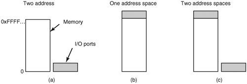
On other computers, I/O registers are part of the regular memory address space, as shown in Fig. 3-3(b). This scheme is called memory-mapped I/O, and was introduced with the PDP-11 minicomputer. Each control register is assigned a unique memory address to which no memory is assigned. Usually, the assigned addresses are at the top of the address space. A hybrid scheme, with memory-mapped I/O data buffers and separate I/O ports for the control registers is shown in Fig. 3-3(c). The Pentium uses this architecture, with addresses 640K to 1M being reserved for device data buffers in IBM PC compatibles, in addition to I/O ports 0 through 64K.
[Page 226] How do these schemes work? In all cases, when the CPU wants to read a word, either from memory or from an I/O port, it puts the address it needs on the address lines of the bus and then asserts a READ signal on a bus control line. A second signal line is used to tell whether I/O space or memory space is needed. If it is memory space, the memory responds to the request. If it is I/O space, the I/O device responds to the request. If there is only memory space [as in Fig. 3-3(b)], every memory module and every I/O device compares the address lines to the range of addresses that it services. If the address falls in its range, it responds to the request. Since no address is ever assigned to both memory and an I/O device, there is no ambiguity and no conflict. 3.1.4. Interrupts Usually, controller registers have one or more status bits that can be tested to determine if an output operation is complete or if new data is available from an input device. A CPU can execute a loop, testing a status bit each time until a device is ready to accept or provide new data. This is called polling or busy waiting. We saw this concept in Sec. 2.2.3 as a possible method to deal with critical sections, and in that context it was dismissed as something to be avoided in most circumstances. In the realm of I/O, where you might have to wait a very long time for the outside world to accept or produce data, polling is not acceptable except for very small dedicated systems not running multiple processes.
[Page 227]In addition to status bits, many controllers use interrupts to tell the CPU when they are ready to have their registers read or written. We saw how interrupts are handled by the CPU in Sec. 2.1.6. In the context of I/O, all you need to know is that most interface devices provide an output which is logically the same as the "operation complete" or "data ready" status bit of a register, but which is meant to be used to drive one of the IRQ (Interrupt ReQuest) lines of the system bus. Thus when an interrupt-enabled operation completes, it interrupts the CPU and starts the interrupt handler running. This piece of code informs the operating system that I/O is complete. The operating system may then check the status bits to verify that all went well, and either harvest the resulting data or initiate a retry. The number of inputs to the interrupt controller may be limited; Pentium-class PCs have only 15 available for I/O devices. Some controllers are hard-wired onto the system parentboard, for example, the disk and keyboard controllers of an IBM PC. On older systems, the IRQ used by the device was set by a switch or jumper associated with the controller. If a user bought a new plug-in board, he had to manually set the IRQ to avoid conflicts with existing IRQs. Few users could do this correctly, which led the industry to develop Plug 'n Play, in which the BIOS can automatically assign IRQs to devices at boot time to avoid conflicts. 3.1.5. Direct Memory Access (DMA) Whether or not a system has memory-mapped I/O, its CPU needs to address the device controllers to exchange data with them. The CPU can request data from an I/O controller one byte at a time but doing so for a device like a disk that produces a large block of data wastes the CPU's time, so a different scheme, called DMA (Direct Memory Access) is often used. The operating system can only use DMA if the hardware has a DMA controller, which most systems do. Sometimes this controller is integrated into disk controllers and other controllers, but such a design requires a separate DMA controller for each device. More commonly, a single DMA controller is available (e.g., on the parentboard) for regulating transfers to multiple devices, often concurrently. No matter where it is physically located, the DMA controller has access to the system bus independent of the CPU, as shown in Fig. 3-4. It contains several registers that can be written and read by the CPU. These include a memory address register, a byte count register, and one or more control registers. The control registers specify the I/O port to use, the direction of the transfer (reading from the I/O device or writing to the I/O device), the transfer unit (byte at a time or word at a time), and the number of bytes to transfer in one burst. Figure 3-4. Operation of a DMA transfer. (This item is displayed on page 228 in the print version) 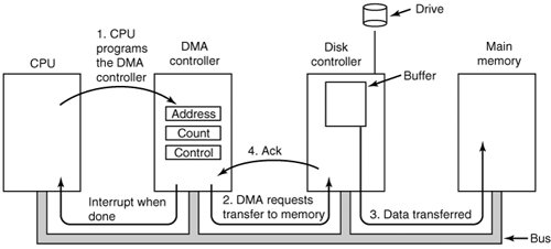
To explain how DMA works, let us first look at how disk reads occur when DMA is not used. First the controller reads the block (one or more sectors) from the drive serially, bit by bit, until the entire block is in the controller's internal buffer. Next, it computes the checksum to verify that no read errors have occurred. Then the controller causes an interrupt. When the operating system starts running, it can read the disk block from the controller's buffer a byte or a word at a time by executing a loop, with each iteration reading one byte or word from a controller device register, storing it in main memory, incrementing the memory address, and decrementing the count of items to be read until it reaches zero.
[Page 228] When DMA is used, the procedure is different. First the CPU programs the DMA controller by setting its registers so it knows what to transfer where (step 1 in Fig. 3-4). It also issues a command to the disk controller telling it to read data from the disk into its internal buffer and verify the checksum. When valid data are in the disk controller's buffer, DMA can begin. The DMA controller initiates the transfer by issuing a read request over the bus to the disk controller (step 2). This read request looks like any other read request, and the disk controller does not know or care whether it came from the CPU or from a DMA controller. Typically, the memory address to write to is on the address lines of the bus so when the disk controller fetches the next word from its internal buffer, it knows where to write it. The write to memory is another standard bus cycle (step 3). When the write is complete, the disk controller sends an acknowledgement signal to the disk controller, also over the bus (step 4). The DMA controller then increments the memory address to use and decrements the byte count. If the byte count is still greater than 0, steps 2 through 4 are repeated until the count reaches 0. At this point the controller causes an interrupt. When the operating system starts up, it does not have to copy the block to memory; it is already there. You may be wondering why the controller does not just store the bytes in main memory as soon as it gets them from the disk. In other words, why does it need an internal buffer? There are two reasons. First, by doing internal buffering, the disk controller can verify the checksum before starting a transfer. If the checksum is incorrect, an error is signaled and no transfer to memory is done.
[Page 229]The second reason is that once a disk transfer has started, the bits keep arriving from the disk at a constant rate, whether the controller is ready for them or not. If the controller tried to write data directly to memory, it would have to go over the system bus for each word transferred. If the bus were busy due to some other device using it, the controller would have to wait. If the next disk word arrived before the previous one had been stored, the controller would have to store it somewhere. If the bus were very busy, the controller might end up storing quite a few words and having a lot of administration to do as well. When the block is buffered internally, the bus is not needed until the DMA begins, so the design of the controller is much simpler because the DMA transfer to memory is not time critical. Not all computers use DMA. The argument against it is that the main CPU is often far faster than the DMA controller and can do the job much faster (when the limiting factor is not the speed of the I/O device). If there is no other work for it to do, having the (fast) CPU wait for the (slow) DMA controller to finish is pointless. Also, getting rid of the DMA controller and having the CPU do all the work in software saves money, important on low-end (embedded) computers. |