Section D.1. SDRAM Basics
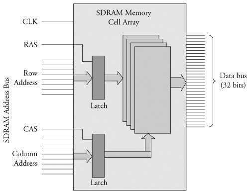
D.1. SDRAM BasicsTo understand SDRAM setup, it is necessary to understand the basics of how an SDRAM device operates. Without going into the details of the hardware design, an SDRAM device is organized as a matrix of cells, with a number of address bits dedicated to row addressing and a number dedicated to column addressing. Figure D-1 illustrates this. Figure D-1. Simplified SDRAM block diagram Inside the memory matrix, the circuitry is quite complex. A simplified example of a read operation is as follows: A given memory location is referenced by placing a row address on the row address lines and then placing a column address on the column address lines. After some time has passed, the data stored at the location addressed by the row and column inputs are made available to the processor on the data bus. The processor outputs a row address on the SDRAM address bus and asserts its Row Address Select (RAS) signal. After a short preprogrammed delay to allow the SDRAM circuitry to capture the row address, the processor outputs a column address and asserts its Column Address Select (CAS) signal. The SDRAM controller translates the actual physical memory address into row and column addresses. Many SDRAM controllers can be configured with the row and column width sizes; the PPC405GP is one of those examples. Later you will see that this must be configured as part of the SDRAM controller setup. This example is much simplified, but the concepts are the same. A burst read, for example, which reads four memory locations at once, outputs a single RAS and CAS cycle, and the internal SDRAM circuitry automatically increments the column address for the subsequent three locations of the burst read, eliminating the need for the processor to issue four separate CAS cycles. This is but one example of performance optimization. The best way to understand this is to absorb the details of an actual memory chip. An example of a well-written data sheet is included in Section D.4.1, "Suggestions for Additional Reading." D.1.1. SDRAM RefreshAn SDRAM is composed of a single transistor and a capacitor. The transistor supplies the charge, and the capacitor's job is to retain (store) the value of the individual cell. For reasons beyond the scope of this discussion, the capacitor can hold the value for only a small duration. One of the fundamental concepts of dynamic memory is that the capacitors representing each cell must be periodically recharged to maintain their value. This is referred to as SDRAM refresh. A refresh cycle is a special memory cycle that neither reads nor writes data to the memory. It simply performs the required refresh cycle. One of the primary responsibilities of an SDRAM controller is to guarantee that refresh cycles are issued in time to meet the chip's requirements. The chip manufacturers specify minimum refresh intervals, and it is the designer's job to guarantee it. Usually the SDRAM controller can be configured directly to select the refresh interval. The PowerPC 405GP presented here has a register specifically for this purpose. We will see this shortly. |
EAN: 2147483647
Pages: 167