28.
11.2 Busing Strategies
One of the most critical design decisions for the data-path is how to connect together its hardware resources. There are three general strategies: point-to-point connections, a single shared bus interconnection, or multiple special-purpose buses. Each represents a trade-off between data-path and control complexity and the amount of parallelism supported by the hardware. This determines the processor's efficiency, defined as the number of control states(or clock cycles) needed to fetch and execute a typical instruction. When a data-path supports many simultaneous transfers among data-path elements, the control unit requires fewer states (and clock cycles) to execute a given instruction.In this section, we will examine methods for organizing the interconnection of data-path components, using the example of four general-purpose registers. We will consider how the data-path can support the operation of a register-to-register swap-that is, simultaneous exchange of the contents of one register with another. In register transfer notation, we write the instruction's execution sequence as
SWAP
(Ri , Rj): Ri --> Rj;
Rj --> Ri;
where Ri and Rj are the registers whose contents are to be swapped.
11.2.1 Point-to-Point Connections
In a point-to-point interconnection scheme, there is a path from every possible source to every possible destination.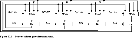
Figure 11.8 shows how this can be implemented for the four-register example using 4-to-1 multi-plexers.
Each of the four registers receives its parallel load inputs from an associated multiplexer block. Ri is an edge-triggered register, which is loaded when the LDi input is asserted. We assume the load signal takes effect only on the appropriate clock edge; that is, it is a synchronous control signal. If each register is N bits wide, the multiplexer blocks must contain N 4-to-1 multiplexers, one multiplexer for each bit in the register. These are controlled by the 2-bit-wide selection inputs, Si<1:0> for register Ri.
Register Transfer Operations and Event Timings To see some of the possible transfers and how they may be implemented, consider the register transfers R1 --> R0 (transfer the contents of R1 to R0) and R2 --> R3 (transfer the contents of R2 to R3). The following detailed register transfer operations describe the necessary sequencing of the control signals:
01 --> S0<1:0>;
10 --> S3<1:0>;
1 --> LD0;
1 --> LD3;
The first two register transfer operations connect R0's input lines to the output of R1, and similarly for R3 being driven from R2. The last two assert the load signals for registers R0 and R3, respectively.
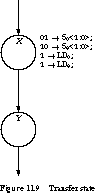
Figure 11.9 shows a state diagram fragment to illustrate when the control signals are asserted and when they take effect. We assume a Moore machine implementation (a synchronous Mealy with registered outputs behaves analogously). When entering state X the multiplexer control signals are asserted, gating R1 and R2 to the inputs of R0 and R3. The state also asserts the R0 and R3 load signals. But because these are synchronous, they do not take effect until the next state transition.
Thus, the R1 and R2 signals have time to propagate through the multiplexer blocks and become stable for the requisite setup times before the clock edge arrives that advances the finite state machine to state Y. The contents of R0 and R3 change on this state transition, not the one that caused the load inputs to become asserted. Since the new values take some time to propagate through the register load circuitry before they emerge at the outputs, the hold time requirements at the register inputs are easily met.
The SWAP Operation To see how the interconnection scheme can implement a SWAP operation, you need to understand the timing relationship between register transfer operations and their effect on the data-path. Consider a SWAP between registers R1 and R2. The control signal settings are
01 --> S2<1:0>;
10 --> S1<1:0>;
1 --> LD2;
1 --> LD1;
On entering state X, the multiplexer selection signals establish the desired pathways between register outputs and inputs. The load signals are asserted, but the registers have not yet received their new values. This occurs only at the clock edge that causes the transition to state Y. Fortunately, the new values appear at the outputs well after the hold time requirements at the inputs have been met.
Discussion The point-to-point scheme is so flexible that it can transfer new values into the four registers at the same time. But there is a significant hardware cost. A 4-to-1 multiplexer requires at least five gates for its implementation (recall Figure 4.29). Assuming a 32-bit-wide data-path, this means 160 gates per register or 640 gates for the four-register example. For this reason, point-to-point connections can only be used in rare cases in which the flexibility far outweighs the implementation cost.
11.2.2 Single Bus
A bus is a set of interconnection pathways that are shared by multiple data sources and destinations. If the point-to-point connection scheme is too hardware intensive, a lower-cost alternative is to use a single interconnection bus. This is shown in Figure 11.10.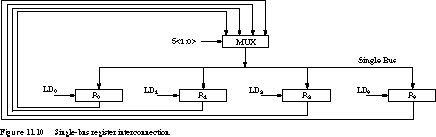
The block with a multiplexer for each register has been replaced by a block with a single multiplexer that is shared by all registers. The hardware cost is 25% of that of the point-to-point approach. The multiplexer places selected data on a bus that feeds the load inputs of all registers.
This dramatic reduction in hardware cost comes at a price: The shared bus (and its multiplexer) is a critical resource because it can be used by only one transfer at a time. However, the single source register can still "broadcast" simultaneously to more than one destination register.
The Register Transfers Revisited To see that transfers now require more states, let's again consider the transfer of R1 to R0 and R2 to R3. These now require two separate states, asserting the following control signals:
State X:(R1 --> R0)
01 --> S<1:0>;
1 --> LD0;
State Y:(R2 --> R3)10 --> S<1:0>;
1 --> LD3;
The SWAP Operation Revisited Since the data-path no longer supports two simultaneous transfers, the register swap operation becomes much more difficult for us to implement. We must stage the data to be swapped through a temporary register that we introduce into the data-path. Let's call the temporary register R4. This means that we have to expand to a 5-to-1 multiplexer.
Swapping the contents of registers R1 and R2 now requires the following register transfer operations:
State X:(R1 --> R4)
001 --> S<2:0>;
1 --> LD4;
State Y:(R2 --> R1)
010 --> S<2:0>;
1 --> LD1;
State Z:(R4 --> R2)
100 --> S<2:0>;
1 --> LD2;
With point-to-point connections, SWAP could be implemented in a single state and just one clock cycle
(we assume one clock cycle per state). Using a single bus interconnection, however, SWAP requires an extra register, a larger MUX, and three control states.Discussion This illustrates a fundamental trade-off in computer hardware: extra complexity in the data-path can reduce the control complexity and vice versa. The correct design decision depends critically on the frequency of operations. If you seldom require multiple simultaneous transfers, your correct choice is the simpler data-path. If you need to SWAP frequently, you should choose the point-to-point method.
A compromise strategy is also possible. It strikes a balance between control and data-path complexity by introducing a small number of additional buses just where they are needed. We will see this in Section 11.2.3.
Multiplexers Versus Tri-State Drivers So far, we have used multiplexers to make connection between sources and destinations. An alternative that dramatically reduces the necessary hardware takes advantage of tri-state or open-collector buffers. Recall that these kinds of circuits allow multiple sources to share the same wire, as long as only one buffer is driving the shared data line at a time.
We show the method, using tri-states, in Figure 11.11.
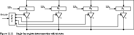
Any of the four registers can be the source for the single bus or be loaded from it. The decoder guarantees that only one of the registers is gated onto the bus through its tri-state buffers. Most packaged logic registers include tri-state devices, so this form of interconnection is convenient.
11.2.3 Multiple Buses
Real data-path designs incorporate the usual engineering trade-offs be-tween control and data-path complexity. Typically, they have more than one bus but less than a full point-to-point scheme. In this subsection, we compare a single-bus scheme to an interconnection arrangement that uses a small number of buses. The metric of comparison we will use is the number of processor states(and clock cycles) it takes to implement a simple instruction.Single-Bus Register Transfer Diagram
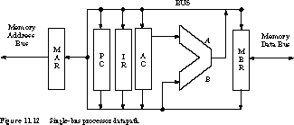
Figure 11.12 gives a simple single-bus design for the processor described in Figure 11.4. The registers are MAR, MBR, PC, IR, and AC, and the only functional unit is the ALU. The AC is hardwired to the A input of the ALU and the MAR is write-only. We call this figure a register transfer diagram because it highlights the way registers and functional units are interconnected.
By examining the data-path, we can quickly determine the register transfer operations it supports:
- Bus as destination: PC --> BUS, IR --> BUS, AC --> BUS,
MBR --> BUS, ALU Result --> BUS;- Bus as source: BUS --> PC, BUS --> IR, BUS --> AC, BUS --> MBR,
BUS --> ALU B, BUS --> MAR;- Hardwired: AC --> ALU A;
- Bus as source: BUS --> PC, BUS --> IR, BUS --> AC, BUS --> MBR,
[X]" which adds the contents of memory location X to the AC and stores the result back into the AC. With the connection scheme of Figure 11.12, the set of register transfer steps to execute the instruction are the following (we group the operations by state and cycle):- Fetch Operand Cycle 1:
IR <operand address> --> BUS;
BUS --> MAR;
- Cycle 2:
Memory Read;
Databus --> MBR;
- Perform ADD Cycle 3:
MBR --> BUS;
BUS --> ALU B;
AC --> ALU A;
ADD;
- Write Result Cycle 4:
ALU Result --> BUS;
BUS --> AC;
Multiple Bus Register Transfer Diagram 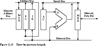
Figure 11.13 gives an alternative three-bus organization that supports higher parallelism in the data-path. More parallelism means that more transfers can take place in the same state. This should lead us to a reduced state and cycle count for the typical instruction.
We partition the single bus functionally into a Memory Bus (MBUS), Result Bus (RBUS), and Address Bus (ABUS). The first connects the MBR with the ALU and IR, the second establishes a pathway between the ALU result and the AC and MBR, and the last provides connections between the IR, PC, and MAR.
Multiple-Bus Cycle-by-Cycle Instruction Execution The cycle-by-cycle register transfer operations now become
- Fetch Operand Cycle 1:
IR <operand address> --> ABUS;
ABUS --> MAR;
- Cycle 2:
Memory Read;
Databus --> MBR;
- Perform ADD
- Cycle 3:
MBR --> MBUS;
MBUS --> ALU B;
AC --> ALU A;
ADD;
- Write Result
- ALU Result --> RBUS;
RBUS --> AC;
[Top] [Next] [Prev]