Chipsets
| We can't talk about modern motherboards without discussing chipsets. The chipset is the motherboard; therefore, any two boards with the same chipsets are functionally identical unless the vendor has added features to those provided by the chipset or removed support for certain chipset features. The chipset usually contains the processor bus interface (called front-side bus, or FSB), memory controllers, bus controllers, I/O controllers, and more. All the circuits of the motherboard are contained within the chipset. If the processor in your PC is like the engine in your car, the chipset represents the chassis. It is the framework in which the engine rests and is its connection to the outside world. The chipset is the frame, suspension, steering, wheels and tires, transmission, drive shaft, differential, and brakes. The chassis in your car is what gets the power to the ground, allowing the vehicle to start, stop, and corner. In the PC, the chipset represents the connection between the processor and everything else. The processor can't talk to the memory, adapter boards, devices, and so on without going through the chipset. The chipset is the main hub and central nervous system of the PC. If you think of the processor as the brain, the chipset is the spine and central nervous system. Because the chipset controls the interface or connections between the processor and everything else, the chipset ends up dictating which type of processor you have; how fast it will run; how fast the buses will run; the speed, type, and amount of memory you can use; and more. In fact, the chipset might be the single most important component in your system, possibly even more important than the processor. I've seen systems with faster processors be outperformed by systems with slower processor but a better chipset, much like how a car with less power might win a race through better cornering and braking. When deciding on a system, I start by choosing the chipset first because the chipset decision then dictates the processor, memory, I/O, and expansion capabilities. Chipset EvolutionWhen IBM created the first PC motherboards, it used several discrete (separate) chips to complete the design. Besides the processor and optional math coprocessor, many other components were required to complete the system. These other components included items such as the clock generator, bus controller, system timer, interrupt and DMA controllers, CMOS RAM and clock, and keyboard controller. Additionally, many other simple logic chips were used to complete the entire motherboard circuit, plus, of course, things such as the actual processor, math coprocessor (floating-point unit), memory, and other parts. Table 4.10 lists all the primary chip components used on the original PC/XT and AT motherboards.
In addition to the processor/coprocessor, a six-chip set was used to implement the primary motherboard circuit in the original PC and XT systems. IBM later upgraded this to a nine-chip design in the AT and later systems, mainly by adding more interrupt and DMA controller chips and the nonvolatile CMOS RAM/Real-Time Clock chip. All these motherboard chip components came from Intel or an Intel-licensed manufacturer, except the CMOS/Clock chip, which came from Motorola. To build a clone or copy of one of these IBM systems required all these chips plus many smaller discrete logic chips to glue the design together, totaling 100 or more individual chips. This kept the price of a motherboard high and left little room on the board to integrate other functions. In 1986, a company called Chips and Technologies introduced a revolutionary component called the 82C206the main part of the first PC motherboard chipset. This was a single chip that integrated into it all the functions of the main motherboard chips in an AT-compatible system. This chip included the functions of the 82284 Clock Generator, 82288 Bus Controller, 8254 System Timer, dual 8259 Interrupt Controllers, dual 8237 DMA Controllers, and even the MC146818 CMOS/Clock chip. Besides the processor, virtually all the major chip components on a PC motherboard could now be replaced by a single chip. Four other chips augmented the 82C206 acting as buffers and memory controllers, thus completing virtually the entire motherboard circuit with five total chips. This first chipset was called the CS8220 chipset by Chips and Technologies. Needless to say, this was a revolutionary concept in PC motherboard manufacturing. Not only did it greatly reduce the cost of building a PC motherboard, but it also made designing a motherboard much easier. The reduced component count meant the boards had more room for integrating other items formerly found on expansion cards. Later, the four chips augmenting the 82C206 were replaced by a new set of only three chips, and the entire set was called the New Enhanced AT (NEAT) CS8221 chipset. This was later followed by the 82C836 Single Chip AT (SCAT) chipset, which finally condensed all the chips in the set down to a single chip. The chipset idea was rapidly copied by other chip manufacturers. Companies such as Acer, Erso, Opti, Suntac, Symphony, UMC, and VLSI each gained an important share of this market. Unfortunately for many of them, the chipset market has been a volatile one, and many of them have long since gone out of business. In 1993, VLSI had become the dominant force in the chipset market and had the vast majority of the market share; by the next year, VLSI (which later was merged into Philips Semiconductors), along with virtually everybody else in the chipset market, was fighting to stay alive. This is because a new chipset manufacturer had come on the scene, and within a year or so of getting serious, it was totally dominating the chipset market. That company was Intel, and after 1994, it had a virtual lock on the chipset market. If you have a motherboard built since 1994 that uses or accepts an Intel processor, chances are good that it has an Intel chipset on it as well. Intel struggled somewhat with chipsets from 1999 through 2001 because of its reliance on RDRAM memory. Intel originally signed a contract with Rambus back in 1996 declaring it would support this memory as its primary focus for desktop PC chipsets through 2001. I suspect this has turned out to be something Intel regrets (the contract has since expired). RDRAM memory had a significantly higher price than DDR SDRAM memory. Consequently, Intel introduced the 845 chipset (code named Brookdale), which supported DDR SDRAM with the Pentium 4. Since that time, all of Intel's Pentium chipsets have supported either DDR or DDR2 memory. Intel is not alone in the Pentium chipset business: VIA Technologies, Silicon Integrated Systems (SiS), ATI, and ULi Electronics (formerly ALi Corporation) all make chipsets for Pentium-based systems. In addition, almost all these chipsets also support SDRAM, DDR-SDRAM, or DD2-SDRAM (although SiS makes a few chipsets that use RDRAM). Although AMD has developed its own chipsets for the K6 and Athlon family of processors, it now emphasizes encouraging third-party chipset developers to support its products. Today, VIA Technologies is the leading developer of chipsets for AMD processors. The popularity of AMD processors has encouraged NVIDIA, SiS, ATI, and ULi Electronics to develop chipsets for AMD-based systems as well. It is interesting to note that the original PC chipset maker, Chips and Technologies, survived by changing course to design and manufacture video chips and found a niche in that market specifically for laptop and notebook video chipsets. Chips and Technologies was subsequently purchased by Intel in 1998 as a part of Intel's video strategy. Intel ChipsetsYou can't talk about chipsets today without discussing Intel because it currently owns the vast majority of the chipset market. It is interesting to note that we probably have Compaq to thank for forcing Intel into the chipset business in the first place! The thing that really started it all was the introduction of the EISA bus designed by Compaq in 1989. At that time, it had shared the bus with other manufacturers in an attempt to make it a market standard. However, Compaq refused to share its EISA bus chipseta set of custom chips necessary to implement this bus on a motherboard. Enter Intel, who decided to fill the chipset void for the rest of the PC manufacturers wanting to build EISA bus motherboards. As is well known today, the EISA bus failed to become a market success except for a short-term niche server business, but Intel now had a taste of the chipset business and this it apparently wouldn't forget. With the introduction of the 286 and 386 processors, Intel became impatient with how long it took the other chipset companies to create chipsets around its new processor designs; this delayed the introduction of motherboards that supported the new processors. For example, it took more than two years after the 286 processor was introduced for the first 286 motherboards to appear and just over a year for the first 386 motherboards to appear after the 386 had been introduced. Intel couldn't sell its processors in volume until other manufacturers made motherboards that would support them, so it thought that by developing motherboard chipsets for a new processor in parallel with the new processor, it could jumpstart the motherboard business by providing ready-made chipsets for the motherboard manufacturers to use. Intel tested this by introducing the 420 series chipsets along with its 486 processor in April 1989. This enabled the motherboard companies to get busy right away, and in only a few months the first 486 motherboards appeared. Of course, the other chipset manufacturers weren't happy; now they had Intel as a competitor, and Intel would always have chipsets for new processors on the market first! Intel then realized that it made both processors and chipsets, which were 90% of the components on a typical motherboard. What better way to ensure that motherboards were available for its Pentium processor when it was introduced than by making its own motherboards as well and having these boards ready on the new processor's introduction date. When the first Pentium processor debuted in 1993, Intel also debuted the 430LX chipset as well as a fully finished motherboard. Now, besides the chipset companies being upset, the motherboard companies weren't too happy, either. Intel was not only the major supplier of parts needed to build finished boards (processors and chipsets), but was now building and selling the finished boards as well. By 1994, Intel dominated the processor and chipset markets and had cornered the motherboard market as well. Now as Intel develops new processors, it develops chipsets and motherboards simultaneously, which means they can be announced and shipped in unison. This eliminates the delay between introducing new processors and waiting for motherboards and systems capable of using them, which was common in the industry's early days. For the consumer, this means no waiting for new systems. Since the original Pentium processor in 1993, we have been able to purchase ready-made systems on the same day a new processor is released. In my seminars, I ask how many people in the class have Intel-brand PCs. Of course, Intel does not sell or market a PC under its own name, so nobody thinks they have an "Intel-brand" PC. But, if your motherboard was made by Intel, for all intents and purposes you sure seem to have an Intel-brand PC, at least as far as the components are concerned. Does it really matter whether the Dells or Gateways of the world put that same Intel motherboard into a slightly different-looking case with their name on it? If you look under the covers, you'll find that many, if not most, of the systems from the major manufacturers are really the same because they basically use the same parts. Although more and more major manufacturers are offering AMD-based systems as alternatives to Intel's, no single manufacturer dominates AMD motherboard sales the way Intel has dominated OEM sales to major system manufacturers. To hold down pricing, many low-cost retail systems based on microATX motherboards use non-Intel motherboards (albeit with Intel chipsets in most cases). But, even though many companies make PC-compatible motherboards for aftermarket upgrades or local computer assemblers, Intel still dominates the major vendor OEM market for midrange and high-end systems. Intel Chipset Model NumbersStarting with the 486 in 1989, Intel began a pattern of numbering its chipsets as shown in Table 4.11.
The chipset numbers listed here are abbreviations of the actual chipset numbers stamped on the individual chips. For example, one of the popular Pentium II/III chipsets was the Intel 440BX chipset, which consisted of two components: the 82443BX North Bridge and the 82371EB South Bridge. Likewise, the 865G chipset supports the Pentium 4 and consists of two main parts: the 82865G graphics memory controller hub (GMCH; replaces the North Bridge and includes integrated video) and an 82801EB or 82801EBR I/O controller hub (ICH5 or ICH5R; replaces the South Bridge). By reading the logo (Intel or others) as well as the part number and letter combinations on the larger chips on your motherboard, you can quickly identify the chipset your motherboard uses. Intel has used two distinct chipset architectures: a North/South Bridge architecture and a newer hub architecture. All its more recent 800 and 900 series chipsets use the hub architecture. Tip In many cases, the North Bridge/GMCH/MCH chip on recent motherboards is covered up with a passive or active heatsink, and some motherboards also use a heatsink on the South Bridge or ICH chip. To determine the chipset used in these systems, watch for motherboard information displayed at system startup by some systems or use a third-party hardware reporting program such as SiSoftware Sandra (download from http://www.sisoftware.co.uk/). Intel Extreme Graphics ArchitectureWith the release of the 845-series chipsets with integrated video (845G-series models, covered later in this chapter), Intel implemented what it called Extreme Graphics Architecture. In its initial version, this architecture supported 3D graphics, featuring the following four technologies aimed at improving 3D rendering speed and quality:
This initial implementation of Extreme Graphics Architecture improved 3D rendering compared to Intel's earlier integrated video chipsets (the 810- and 815-series chipsets, which have limited 3D functions), but its performance and features still lagged behind even the mid-range dedicated graphics cards of the time (such as NVIDIA's GeForce 2 MX 200). Intel later added more feature support when it released the Extreme Graphics Architecture 2. However, it wasn't until the third time aroundwhen Intel renamed it the Graphics Media Accelerator 900that it added support for most of the core 3D features made standard in DirectX 9. The Graphics Media Accelerator 900, though, lacks support for vertex shaders. The 900 was included in the 915 family of Intel chipsets. The most recent iteration is the Intel Graphics Media Accelerator 950, which is a faster version of the 900 and is found in Intel's 945 chipset family. GMA 950 offers a 400MHz clock speed, compared to 333MHz for GMA 900, and features support for 16:9 wide-screen flat panels, motion compensation for DVD playback, HDTV playback (720p and 1080i), digital TV support, and DirectX 9.0 vertex shader 3.0 and T&L software support.
AMD ChipsetsAMD took a gamble with its Athlon family of processors. With these processors, AMD decided for the first time to create a chip that was Intel compatible with regard to software but not directly hardware or pin compatible. Whereas the K6 series would plug into the same Socket 7 that Intel designed for the Pentium processor line, the AMD Athlon and Duron would not be pin compatible with the Pentium II/III and Celeron chips. This also meant that AMD could not take advantage of the previously existing chipsets and motherboards when the Athlon and Duron were introduced; instead, AMD would have to either create its own chipsets and motherboards or find other companies who would. The gamble has paid off. AMD bootstrapped the market by introducing its own chipset, referred to as the AMD-750 chipset (code named Irongate). The AMD 750 chipset consists of the 751 System Controller (North Bridge) and the 756 Peripheral Bus Controller (South Bridge). AMD followed with the AMD-760 chipset for the Athlon/Duron processors, which was the first major chipset on the market supporting DDR SDRAM for memory. It consists of two chipsthe AMD-761 System Bus Controller (North Bridge) and the AMD-766 Peripheral Bus Controller (South Bridge). Similarly, AMD established a new standard chipset architecture for its line of 64-bit processorsthe Athlon 64 and Opteronby developing the AMD-8000 chipset. AMD's pioneering efforts have inspired other companies, such as VIA Technologies, NVIDIA, Ali, and SiS, to develop chipsets specifically designed to interface with AMD processors utilizing (over time) Slot A, Socket A, Socket 754, Socket 939, and Socket 940. In the latter half of 2006, expect Socket M2 to join this list. This has enabled the motherboard companies to make a variety of boards supporting these chips and the Athlon family of processors to take a fair amount of market share away from Intel in the process. Traditional North/South Bridge ArchitectureMost of Intel's earlier chipsets (and, until a few years ago, virtually all non-Intel chipsets) are broken into a multitiered architecture incorporating what are referred to as North and South Bridge components, as well as a Super I/O chip:
Figure 4.30 shows a typical AMD Socket A motherboard using North/South Bridge architecture with the locations of all chips and components. Figure 4.30. A typical Socket A (AMD Athlon/Duron) motherboard showing component locations.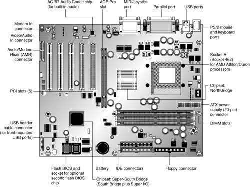 The North Bridge is sometimes referred to as the PAC (PCI/AGP Controller). It is essentially the main component of the motherboard and is the only motherboard circuit besides the processor that normally runs at full motherboard (processor bus) speed. Most modern chipsets use a single-chip North Bridge; however, some of the older ones actually consisted of up to three individual chips to make up the complete North Bridge circuit. The South Bridge is the lower-speed component in the chipset and has always been a single individual chip. The South Bridge is a somewhat interchangeable component in that different chipsets (North Bridge chips) often are designed to use the same South Bridge component. This modular design of the chipset allows for lower cost and greater flexibility for motherboard manufacturers. Similarly, many vendors produce several versions of pin-compatible South Bridge chips with different features to enable more flexible and lower-cost manufacturing and design. The South Bridge connects to the 33MHz PCI bus and contains the interface or bridge to the 8MHz ISA bus (if present). It also typically contains dual ATA/IDE hard disk controller interfaces, one or more USB interfaces, and in later designs even the CMOS RAM and real-time clock functions. In older designs, the South Bridge contained all the components that make up the ISA bus, including the interrupt and DMA controllers. The third motherboard component, the Super I/O chip, is connected to the 8MHz ISA bus or the low pin count (LPC) bus and contains all the standard peripherals that are built in to a motherboard. For example, most Super I/O chips contain the serial ports, parallel port, floppy controller, and keyboard/mouse interface. Optionally, they might contain the CMOS RAM/Clock, IDE controllers, and game port interface as well. Systems that integrate IEEE 1394 and SCSI ports use separate chips for these port types. Most recent motherboards that use North/South Bridge chipset designs incorporate a Super-South Bridge, which incorporates the South Bridge and Super I/O functions into a single chip. Hub ArchitectureThe 800 and 900 series chips from Intel use hub architectures in which the former North Bridge chip is now called a Memory Controller Hub (MCH) and the former South Bridge is called an I/O Controller Hub (ICH). Systems that include integrated graphics use a Graphics Memory Controller Hub (GMCH) in place of the standard MCH. Rather than connect them through the PCI bus as in a standard North/South Bridge design, they are connected via a dedicated hub interface that is twice as fast as PCI. The hub design offers several advantages over the conventional North/South Bridge design:
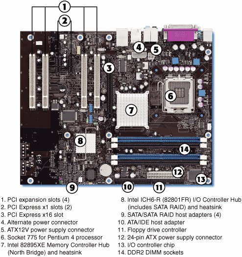
This hub interface design allows for a much greater throughput for PCI devices because there is no South Bridge chip (also carrying traffic from the Super I/O chip) hogging the PCI bus. Due to bypassing PCI, hub architecture also enables greater throughput for devices directly connected to the I/O Controller Hub (formerly the South Bridge), such as the higher-speed ATA-100, Serial ATA, and USB 2.0 interfaces. The hub interface design is also very economical, being only 8 bits wide. Although this seems too narrow to be useful, there is a reason for the design. By making the interface only 8 bits wide, it uses only 15 signals, compared to the 64 signals required by the 32-bit-wide PCI bus interface used by North/South Bridge chip designs. The lower pin count means less circuit routing exists on the board, less signal noise and jitter occur, and the chips themselves have many fewer pins, making them smaller and more economical to produce. Although it transfers only 8 bits at a time, the hub interface executes four transfers per cycle and cycles at 66MHz. This gives it an effective throughput of 4x66MHzx1 byte = 266MB per second (MBps). This is twice the bandwidth of PCI, which is 32 bits wide but runs only one transfer per 33MHz cycles for a total bandwidth of 133MBps. So, by virtue of a very narrowbut very fastdesign, the hub interface achieves high performance with less cost and more signal integrity than with the previous North/South Bridge design. The MCH interfaces between the high-speed processor bus (800/533/400/133/100/66MHz) and the hub interface (66MHz) and AGP bus (533/266/133/66MHz), whereas the ICH interfaces between the hub interface (66MHz) and the ATA (IDE) ports (66/100MHz), the SATA ports on the ICH5 (150MHz), and the PCI bus (33MHz). The ICH also includes a new low-pin-count (LPC) bus, consisting basically of a stripped 4-bit wide version of PCI designed primarily to support the motherboard ROM BIOS and Super I/O chips. By using the same 4 signals for data, address, and command functions, only 9 other signals are necessary to implement the bus, for a total of only 13 signals. This dramatically reduces the number of traces connecting the ROM BIOS chip and Super I/O chips in a system as compared to the 98 ISA bus signals necessary for older North/South Bridge chipsets that used ISA as the interface to those devices. The LPC bus has a maximum bandwidth of 16.67MBps, which is much faster than ISA and more than enough to support devices such as ROM BIOS and Super I/O chips The 9xx series of chipsets uses a second-generation hub design with a new interconnect technology called direct media interface (DMI). DMI runs at 1GBps, or four times faster than the advanced hub architecture (AHA) used by most Intel 8xx-series chipsets or the updated hub interface 1.5 (HI 1.5) used by the 865/875 chipsets. Figure 4.31 shows a typical Intel motherboard that uses bus architecturethe Intel D925XBC, which supports the Intel Pentium 4 and Pentium Extreme Edition processors. Unlike some of Intel's less-expensive hub-based motherboards, the Intel D925XECV2's 925XE chipset doesn't incorporate video. Figure 4.31. Intel's D925XBC motherboard showing component locations. Illustration courtesy of Intel Corporation. High-Speed North-South Bridge ConnectionsIntel is not alone in replacing the slow PCI bus connection between North and South Bridgetype chips with a faster architecture that bypasses the PCI bus. Other companies that have introduced high-speed chipset interconnects include
Table 4.12 compares the performance features and chipset support of major non-Intel high-speed chipset architectures.
Let's examine the popular chipsets, starting with those used in 486 motherboards and working all the way through to the latest Pentium III/Celeron, Pentium 4, Athlon XP, and Athlon 64 chipsets. |
EAN: 2147483647
Pages: 283