P4 (486) Fourth-Generation Processors
| The third generation had been a large change from the previous generations of processors. With the fourth generation, more refinement than complete redesign was accomplished. Even so, Intel, AMD, and others managed to literally double processor performance with their fourth-generation processors. The following section defines the fourth-generation processors from Intel, AMD, and others. 486 ProcessorsIn the race for more speed, the Intel 80486 (normally abbreviated as 486) was another major leap forward. The additional power available in the 486 fueled tremendous growth in the software industry. Tens of millions of copies of Windows, and millions of copies of OS/2, have been sold largely because the 486 finally made the GUI of Windows and OS/2 a realistic option for people who work on their computers every day. Four main features make a given 486 processor roughly twice as fast as an equivalent MHz 386 chip. These features are
The 486 chip is about twice as fast as the 386, so a 386DX-40 is about as fast as a 486SX-20. This made the 486 a much more desirable option, primarily because it could more easily be upgraded to a DX2 or DX4 processor at a later time. You can see why the arrival of the 486 rapidly killed off the 386 in the marketplace. Most of the 486 chips were offered in a variety of maximum speed ratings, varying from 16MHz up to 133MHz. Additionally, 486 processors have slight differences in overall pin configurations. The DX, DX2, and SX processors have a virtually identical 168-pin configuration, whereas the OverDrive chips have either the standard 168-pin configuration or a specially modified 169-pin OverDrive (sometimes also called 487SX) configuration. If your motherboard has two sockets, the primary one likely supports the standard 168-pin configuration, and the secondary (OverDrive) socket supports the 169-pin OverDrive configuration. Most of the later 486-based motherboards with a single ZIF socket support any of the 486 processors except the DX4. The DX4 is different because it requires 3.3V to operate instead of 5V, like most other chips up to that time. A processor rated for a given speed always functions at any of the lower speeds. A 100MHz-rated 486DX4 chip, for example, runs at 75MHz if it is plugged into a 25MHz motherboard. Note that the DX2/OverDrive processors operate internally at two times the motherboard clock rate, whereas the DX4 processors operate at two, two-and-one-half, or three times the motherboard clock rate. Table 3.24 shows the various speed combinations that can result from using the DX2 or DX4 processors with different motherboard clock speeds.
The internal multiplier of the DX4 processor is controlled by the CLKMUL (clock multiplier) signal at pin R-17 (Socket 1) or S-18 (Socket 2, 3, or 6). In most cases, one or two jumpers will be on the board near the processor socket to control the settings for these pins. The motherboard documentation should cover these settings if they can be changed. One interesting capability here is to run the DX4-100 chip in a doubled mode with a 50MHz motherboard speed. This gives you a very fast memory bus, along with the same 100MHz processor speed, as if you were running the chip in a 33/100MHz tripled mode. Many VL-Bus motherboards can run the VL-Bus slots in a buffered mode, add wait states, or even selectively change the clock only for the VL-Bus slots to keep them compatible. In most cases, they don't run properly at 50MHz. Consult your motherboardor even better, your chipset documentationto see how your board is set up. Caution When upgrading an existing system, you should be sure that your socket supports the chip you are installing. This was especially true when putting a DX4 processor in an older system. In that scenario, you needed some type of adapter to regulate the voltage down to 3.3V. Putting the DX4 in a 5V socket destroys the chip! See the earlier section on processor sockets for more information. 486DX ProcessorsThe original Intel 486DX processor was introduced on April 10, 1989, and systems using this chip first appeared during 1990. The first chips had a maximum speed rating of 25MHz; later versions of the 486DX were available in 33MHz- and 50MHz-rated versions. The 486DX originally was available only in a 5V, 168-pin PGA version, but later became available in 5V, 196-pin plastic quad flat pack (PQFP) and 3.3V, 208-pin small quad flat pack (SQFP). These latter form factors were available in SL enhanced versions, which were intended primarily for portable or laptop applications in which saving power is important. Two main features separate the 486 processor from its predecessors:
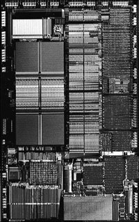
The 486DX processor was fabricated with low-power CMOS technology. The chip has a 32-bit internal register size, a 32-bit external data bus, and a 32-bit address bus. These dimensions are equal to those of the 386DX processor. The internal register size is where the "32-bit" designation used in advertisements comes from. The 486DX chip contains 1.2 million transistors on a piece of silicon no larger than your thumbnail. This figure is more than four times the number of components on 386 processors and should give you a good indication of the 486 chip's relative power. The die for the 486 is shown in Figure 3.37. Figure 3.37. 486 processor die. Photograph used by permission of Intel Corporation. The standard 486DX contains a processing unit, floating-point unit (math coprocessor), memory-management unit, and cache controller with 8KB of internal-cache RAM. Due to the internal cache and a more efficient internal processing unit, the 486 family of processors can execute individual instructions in an average of only 2 processor cycles. Compare this figure with the 286 and 386 families, both of which execute an average 4.5 cycles per instruction. Compare it also with the original 8086 and 8088 processors, which execute an average 12 cycles per instruction. At a given clock rate (MHz), therefore, a 486 processor is roughly twice as efficient as a 386 processor; a 16MHz 486SX is roughly equal to a 33MHz 386DX system; and a 20MHz 486SX is equal to a 40MHz 386DX system. Any of the faster 486s are way beyond the 386 in performance. The 486 is fully instruction-setcompatible with previous Intel processors, such as the 386, but offers several additional instructions (most of which have to do with controlling the internal cache). Similar to the 386DX, the 486 can address 4GB of physical memory and manage as much as 64TB of virtual memory. The 486 fully supports the three operating modes introduced in the 386: real mode, protected mode, and virtual real mode:
The 486DX series has a built-in math coprocessor that sometimes is called an MCP (math coprocessor) or FPU. This series is unlike previous Intel CPU chips, which required you to add a math coprocessor if you needed faster calculations for complex mathematics. The FPU in the 486DX series is 100% software-compatible with the external 387 math coprocessor used with the 386, but it delivers more than twice the performance. It runs in synchronization with the main processor and executes most instructions in half as many cycles as the 386. 486SLThe 486SL was a short-lived, standalone chip. The SL enhancements and features became available in virtually all the 486 processors (SX, DX, and DX2) in what are called SL enhanced versions. SL enhancement refers to a special design that incorporates special power-saving features. The SL enhanced chips originally were designed to be installed in laptop or notebook systems that run on batteries, but they found their way into desktop systems, as well. The SL-enhanced chips featured special power-management techniques, such as sleep mode and clock throttling, to reduce power consumption when necessary. These chips were available in 3.3V versions, as well. Intel designed a power-management architecture called system management mode (SMM). This mode of operation is totally isolated and independent from other CPU hardware and software. SMM provides hardware resources such as timers, registers, and other I/O logic that can control and power down mobile-computer components without interfering with any of the other system resources. SMM executes in a dedicated memory space called system management memory, which is not visible and does not interfere with operating system and application software. SMM has an interrupt called system management interrupt (SMI), which services power-management events and is independent fromand a higher priority thanany of the other interrupts. SMM provides power management with flexibility and security that were not available previously. For example, an SMI occurs when an application program tries to access a peripheral device that is powered down for battery savings, which powers up the peripheral device and re-executes the I/O instruction automatically. Intel also designed a feature called Suspend/Resume in the SL processor. The system manufacturer can use this feature to provide the portable computer user with instant on-and-off capability. An SL system typically can resume (instant on) in 1 second from the suspend state (instant off) to exactly where it left off. You do not need to reboot, load the operating system, or load the applications and their data. Instead, simply push the Suspend/Resume button and the system is ready to go. The SL CPU was designed to consume almost no power in the suspend state. This feature means that the system can stay in the suspend state possibly for weeks and yet start up instantly right where it left off. An SL system can keep working data in normal RAM memory safe for a long time while it is in the suspend state, but saving to a disk still is prudent. 486SXThe 486SX, introduced in April 1991, was designed to be sold as a lower-cost version of the 486. The 486SX is virtually identical to the full DX processor, but the chip does not incorporate the FPU or math coprocessor portion. As you read earlier in this chapter, the 386SX was a scaled-down (some people would say crippled) 16-bit version of the full-blown 32-bit 386DX. The 386SX even had a completely different pinout and was not interchangeable with the more powerful DX version. The 486SX, however, is a different story. The 486SX is, in fact, a full-blown 32-bit 486 processor that is basically pin compatible with the DX. A few pin functions are different or rearranged, but each pin fits into the same socket. The 486SX chip was more a marketing quirk than new technology. Early versions of the 486SX chip actually were DX chips that showed defects in the math-coprocessor section. Instead of being scrapped, the chips were packaged with the FPU section disabled and sold as SX chips. This arrangement lasted for only a short time; thereafter, SX chips got their own mask, which is different from the DX mask. (A mask is the photographic blueprint of the processor and is used to etch the intricate signal pathways into a silicon chip.) The transistor count dropped to 1.185 million (from 1.2 million) to reflect this new mask. The 486SX was available in 16MHz-, 20MHz-, 25MHz-, and 33MHz-rated speeds, and a 486 SX/2 was also available that ran at up to 50MHz or 66MHz. The 486SX typically was made in a 168-pin version, although other surface-mount versions were manufactured in SL-enhanced models. Despite what Intel's marketing and sales information implies, no technical provision exists for adding a separate math coprocessor to a 486SX system; neither was a separate math coprocessor chip ever available to plug in. Instead, Intel wanted you to add a new 486 processor with a built-in math unit and disable the SX CPU that already was on the motherboard. 487SXThe 487SX math coprocessor, as Intel called it, really is a complete 25MHz 486DX CPU with an extra pin added and some other pins rearranged. When the 487SX is installed in the extra socket provided in a 486SX CPU-based system, the 487SX turns off the existing 486SX via a new signal on one of the pins. The extra key pin actually carries no signal itself and exists only to prevent improper orientation when the chip is installed in a socket. The 487SX takes over all CPU functions from the 486SX and also provides math coprocessor functionality in the system. At first glance, this setup seems rather strange and wasteful, so perhaps further explanation is in order. Fortunately, the 487SX turned out to be a stopgap measure while Intel prepared its real surprise: the OverDrive processor. The DX2/OverDrive speed-doubling chips, which are designed for the 487SX 169-pin socket, have the same pinout as the 487SX. These upgrade chips are installed in exactly the same way as the 487SX; therefore, any system that supports the 487SX also supports the DX2/OverDrive chips. Originally, Intel discouraged users from removing the existing chip from the socket and replacing it with a 487SX (or even a DX or DX2/OverDrive). Instead, Intel recommended that PC manufacturers include a dedicated upgrade (OverDrive) socket in their systems because several risks were involved in removing the original CPU from a standard socket. (The following section elaborates on those risks.) Later Intel recommendedor even insisted onthe use of a single processor socket of a ZIF design, which makes upgrading an easy task physically.
DX2/OverDrive and DX4 ProcessorsOn March 3, 1992, Intel introduced the DX2 speed-doubling processors. On May 26, 1992, Intel announced that the DX2 processors also would be available in a retail version called OverDrive. Originally, the OverDrive versions of the DX2 were available only in 169-pin versions, which meant that they could be used only with 486SX systems that had sockets configured to support the rearranged pin configuration. On September 14, 1992, Intel introduced 168-pin OverDrive versions for upgrading 486DX systems. These processors could be added to existing 486 (SX or DX) systems as an upgrade, even if those systems did not support the 169-pin configuration. When you use this processor as an upgrade, you install the new chip in your system, which subsequently runs twice as fast. The DX2/OverDrive processors run internally at twice the clock rate of the host system. If the motherboard clock is 25MHz, for example, the DX2/OverDrive chip runs internally at 50MHz; likewise, if the motherboard is a 33MHz design, the DX2/OverDrive runs at 66MHz. The DX2/OverDrive speed doubling has no effect on the rest of the system; all components on the motherboard run the same as they do with a standard 486 processor. Therefore, you do not have to change other components (such as memory) to accommodate the double-speed chip. The DX2/OverDrive chips have been available in several speeds. Three speed-rated versions have been offered:
Notice that these ratings indicate the maximum speed at which the chip is capable of running. You could use a 66MHz-rated chip in place of the 50MHz- or 40MHz-rated parts with no problem, although the chip will run only at the slower speeds. The actual speed of the chip is double the motherboard clock frequency. When the 40MHz DX2/OverDrive chip is installed in a 16MHz 486SX system, for example, the chip functions only at 32MHzexactly double the motherboard speed. Intel originally stated that no 100MHz DX2/OverDrive chip would be available for 50MHz systemswhich technically has not been true because the DX4 could be set to run in a clock-doubled mode and used in a 50MHz motherboard (see the discussion of the DX4 processor in this section). The only part of the DX2 chip that doesn't run at double speed is the bus interface unit, a region of the chip that handles I/O between the CPU and the outside world. By translating between the differing internal and external clock speeds, the bus interface unit makes speed doubling transparent to the rest of the system. The DX2 appears to the rest of the system to be a regular 486DX chip, but one that seems to execute instructions twice as fast. DX2/OverDrive chips are based on the 0.8-micron circuit technology that was first used in the 50MHz 486DX. The DX2 contains 1.2 million transistors in a three-layer form. The internal 8KB cache, integer, and floating-point units all run at double speed. External communication with the PC runs at normal speed to maintain compatibility. Besides upgrading existing systems, one of the best parts of the DX2 concept was the fact that system designers could introduce very fast systems by using cheaper motherboard designs, rather than the more costly designs that would support a straight high-speed clock. Therefore, a 50MHz 486DX2 system was much less expensive than a straight 50MHz 486DX system. The system board in a 486DX-50 system operates at a true 50MHz. The 486DX2 CPU in a 486DX2-50 system operates internally at 50MHz, but the motherboard operates at only 25MHz. You might be thinking that a true 50MHz DX processorbased system still would be faster than a speed-doubled 25MHz system, and this generally is true. But, the differences in speed actually are very slighta real testament to the integration of the 486 processor and especially to the cache design. When the processor has to go to system memory for data or instructions, for example, it must do so at the slower motherboard operating frequency (such as 25MHz). Because the 8KB internal cache of the 486DX2 has a hit rate of 90%95%, however, the CPU must access system memory only 5%10% of the time for memory reads. Therefore, the performance of the DX2 system can come very close to that of a true 50MHz DX system and cost much less. Even though the motherboard runs at only 33.33MHz, a system with a DX2 66MHz processor ends up being faster than a true 50MHz DX system, especially if the DX2 system has a good L2 cache. Many 486 motherboard designs also include a secondary cache that is external to the cache integrated into the 486 chip. This external cache allows for much faster access when the 486 chip calls for external-memory access. The size of this external cache can vary anywhere from 16KB to 512KB or more. When you add a DX2 processor, an external cache is even more important for achieving the greatest performance gain. This cache greatly reduces the wait states the processor must add when writing to system memory or when a read causes an internal cache miss. For this reason, some systems perform better with the DX2/OverDrive processors than others, usually depending on the size and efficiency of the external-memory cache system on the motherboard. Systems that have no external cache still enjoy a near-doubling of CPU performance, but operations that involve a great deal of memory access are slower. Although the standard DX4 technically was not sold as a retail part, it could be purchased from several vendors, along with the 3.3V voltage adapter needed to install the chip in a 5V socket. These adapters have jumpers that enable you to select the DX4 clock multiplier and set it to 2x, 2.5x, or 3x mode. In a 50MHz DX system, you could install a DX4/voltage-regulator combination set in 2x mode for a motherboard speed of 50MHz and a processor speed of 100MHz! Although you might not be able to take advantage of certain VL-Bus adapter cards, you will have one of the fastest 486-class PCs available. Intel also sold a special DX4 OverDrive processor that included a built-in voltage regulator and heatsink that are specifically designed for the retail market. The DX4 OverDrive chip is essentially the same as the standard 3.3V DX4 with the main exception that it runs on 5V because it includes an on-chip regulator. Also, the DX4 OverDrive chip runs only in the tripled speed mode, and not the 2x or 2.5x modes of the standard DX4 processor. Intel OverDrive products were discontinued several years ago, as were third-party equivalents. Pentium OverDrive for 486SX2 and DX2 SystemsThe Pentium OverDrive Processor became available in 1995. An OverDrive chip for 486DX4 systems had been planned, but poor marketplace performance of the SX2/DX2 chip resulted in it never seeing the light of day. One thing to keep in mind about the 486 Pentium OverDrive chip is that although it was intended primarily for SX2 and DX2 systems, it should work in any upgradeable 486SX or DX system that has a Socket 2 or Socket 3. If you want to install one in an older system, you can check Intel's online upgrade guide for compatibility, located at http://support.intel.com/support/processors/overdrive/. The Pentium OverDrive processor is designed for systems that have a processor socket that follows the Intel Socket 2 specification. This processor also works in systems that have a Socket 3 design, although you should ensure that the voltage is set for 5V rather than 3.3V. The Pentium OverDrive chip includes a 32KB internal L1 cache and the same superscalar (multiple instruction path) architecture of the real Pentium chip. Besides a 32-bit Pentium core, these processors feature increased clock-speed operation due to internal clock multiplication and incorporate an internal write-back cache (standard with the Pentium). If the motherboard supports the write-back cache function, increased performance is realized. Unfortunately, most motherboards, especially older ones with the Socket 2 design, support only write-through cache. Most tests of these OverDrive chips show them to be only slightly ahead of the DX4-100 and behind the DX4-120 and true Pentium 60, 66, or 75. Based on the relative affordability of low-end "real" Pentiums (in their day), it was hard not to justify making the step up to a Pentium system. AMD 486 (5x86)AMD made a line of 486-compatible chips that installed into standard 486 motherboards. In fact, AMD made the fastest 486 processor available, which it called the Am5x86(TM)-P75. The name was a little misleading because the 5x86 part made some people think that this was a fifth-generation Pentium-type processor. In reality, it was a fast clock-multiplied (4x clock) 486 that ran at four times the speed of the 33MHz 486 motherboard you plugged it into. The 5x86 offered high-performance features such as a unified 16KB write-back cache and 133MHz core clock speed; it was approximately comparable to a Pentium 75, which is why it was denoted with a P-75 in the part number. It was the ideal choice for cost-effective 486 upgrades, where changing the motherboard is difficult or impossible. Not all 486 motherboards support the 5x86. The best way to verify that your motherboard supports the chip is by checking with the documentation that came with the board. Look for keywords such as "Am5X86," "AMD-X5," "clock-quadrupled," "133MHz," or other similar wording. Another good way to determine whether your motherboard supports the AMD 5x86 is to look for it in the listed models on AMD's website. There are a few things to note when installing a 5x86 processor into a 486 motherboard:
In addition to the 5x86, the AMD-enhanced 486 product line included 80MHz; 100MHz; and 120MHz CPUs. These are the A80486DX2-80SV8B (40MHzx2), A80486DX4-100SV8B (33MHzx3), and A80486DX4-120SV8B (40MHzx3). Cyrix/TI 486The Cyrix 486DX2/DX4 processors were available in 100MHz, 80MHz, 75MHz, 66MHz, and 50MHz versions. Similar to the AMD 486 chips, the Cyrix versions are fully compatible with Intel's 486 processors and work in most 486 motherboards. The Cx486DX2/DX4 incorporates an 8KB write-back cache, an integrated floating-point unit, advanced power management, and SMM, and was available in 3.3V versions. Note TI originally made all the Cyrix-designed 486 processors, and under the agreement it also sold them under the TI name. They are essentially the same as the Cyrix chips. |
EAN: 2147483647
Pages: 283
- Integration Strategies and Tactics for Information Technology Governance
- An Emerging Strategy for E-Business IT Governance
- Assessing Business-IT Alignment Maturity
- Linking the IT Balanced Scorecard to the Business Objectives at a Major Canadian Financial Group
- Measuring and Managing E-Business Initiatives Through the Balanced Scorecard