6.4 Clock Accuracy Considerations
| | ||
| | ||
| | ||
6.4 Clock Accuracy Considerations
As mentioned above, there are a number of different considerations concerning clock accuracy and the importance of stability that apply at different points in the signal chain. There is the accuracy of the audio sample clock used for A/D and D/A conversion, which will have a direct effect on sound quality, and there is the accuracy of the external reference signal. There is also the question of timing stability in digital audio signals that have travelled over interconnects such as those described in this book, which may have suffered distortions of various kinds. Because the audio sample clock used for conversion in externally synchronized systems must be locked in some way either to the digital audio input clock or the sync reference, it is common for instabilities in either of these signals to affect the stability of the audio sample clock (although they need not). This depends on how the clock is extracted from the digital input signal and the nature of the timing error. Furthermore, clock instability resulting from distortion and interference in the digital interface makes the signal more difficult to decode.
6.4.1 Causes and Effects of Jitter on the Interface Signal
Timing irregularities may arise in signals transferred over a digital audio interface due to a number of factors. These may include bandwidth limitations of the interconnect and the effects of induced noise and other signals. Furthermore, the transmitted signal may already have some jitter, either because the source did not properly reject incoming jitter from an input signal, or because its own free-running clock was unstable. AES3 originally specified that data transitions on the interface should occur within 20 ns of an ideal jitter-free clock. In real products it is normal for interface transition jitter to be well below 20 ns, but when devices which pass on input jitter to their digital outputs are cascaded it is possible for specifications to exceed this value after a number of stages. The degree to which a device passes on jitter is known as its jitter transfer function.
AES3-1997 is somewhat more specific in relation to jitter, specifying limits for output jitter, intrinsic jitter, jitter gain and input jitter tolerance. Output jitter is the sum of the intrinsic jitter of the device's output and that passed through from any timing reference. The intrinsic jitter is specified to be no greater than 0.025UI (unit interval) when measured using a standard high-pass measurement filter specified in the standard. A UI is specified as the smallest timing unit in the interface and there are 128UIs per frame (the modulation method can involve transitions in the middle of a bit cell ). Sinusoidal jitter gain (the ratio of jitter amplitude at the output of the device to that present at the sync signal input) should be no greater than 2dB, again measured using a standard filter. Input jitter tolerance (the maximum jitter value below which a device should correctly decode input data) is specified as 0.25UI peak-to-peak above 8kHz rising to 10UI below 200Hz.
The received signal from a standard two-channel AES interface will have an eye pattern that depends on amplitude and timing irregularities (see Chapter 4). Amplitude errors will close the eye vertically and timing errors will close it horizontally. The limits for correct decoding are laid out in the specification of the interface. Nonetheless, some receivers are better than others at decoding data with a poor eye pattern and this has partly to do with the frequency response of the phase-locked loop in the receiver and its lock-in range (see below). It also depends on the part of the signal from which the decoder extracts its clock, since some transitions are decidedly more unstable than others when the link is poor. Decoders that are very tolerant of poor input signals may at the same time be bad at rejecting jitter. Although they may decode the signal, the resulting sound quality may be poor if the signal is converted within the device without further rejection of jitter and the device may pass on excessive jitter at its output.
Dunn 4 and Dunn and Hawksford 6 have both carried out simulations of the effects of link bandwidth reduction on standard two-channel interface signals. The important conclusions of their work are as follows . When a link suffers high-frequency loss there will be a reduction in amplitude of the shorter pulses and a slowing in rise and fall times at transitions, the effect of which is to delay the zero- crossing transition after short pulses less than the delay after longer pulses . This variable delay is effectively jitter and is solely a result of high-frequency loss. Figure 6.4 shows the HF loss model which was used in both studies (which, although simplistic, is considered a good starting point for analysis), the time constant of which is RC . Figure 6.5 shows a comparison between simulated bi-phase mark data at time constants of 200 ns and 50 ns, showing clearly that at 200 ns the shorter pulses are more attenuated than the longer (a time constant of 200 ns corresponds to a roll-off of -3 dB at 0.8 MHz, whereas 50 ns corresponds to a similar roll-off at around 3.18 MHz). Dunn's results show clearly that for links with a bandwidth of less than around 3 MHz the jitter suffered by transitions in the main part of the AES subframe (the audio data time slots) is far greater than that suffered by the penultimate transition of the Y preamble, as shown in Figure 6.6. Dunn and Hawksford also provide convincing evidence that the jitter is highly correlated with the audio signal and is affected by the difference between the number of zeros and ones in the signal. This situation clearly becomes more critical at higher data rates than those originally specified.
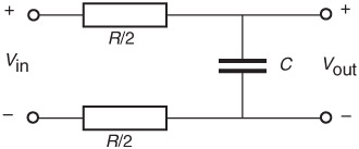
Figure 6.4: High-frequency loss model used in simulating the effects of cables.
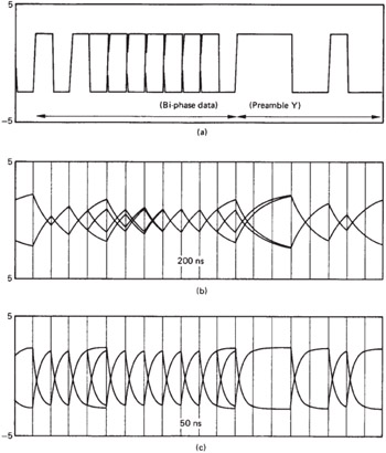
Figure 6.5: A simulation of the effects of high-frequency loss on an AES3-format signal. At (a) the original signal is shown (both polarities are superimposed for clarity), whilst (b) and (c) show the data waveform at link time constants of 200 ns and 50 ns respectively. (Reproduced from J. Dunn, with permission.)
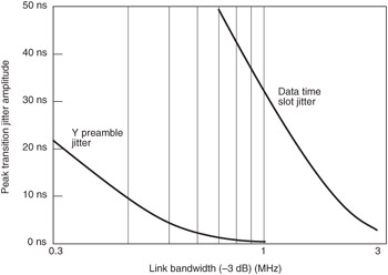
Figure 6.6: Effect of link bandwidth on preamble and data time slot jitter, showing how the Y preamble is affected much less by reduced bandwidth than the data edges. (Reproduced from J. Dunn, with permission.)
6.4.2 Audio Sampling Frequency
It is important to separate the discussion of long-term sample frequency accuracy from stability in the short term. Short-term instability is called 'jitter' and long- term inaccuracy would manifest itself as drift (if in one direction only), or wow and flutter (if cyclically modulated) in extreme cases. Jitter will be covered in the next section.
For professional equipment, the nominal sampling frequency should be accurate to within 10 ppm if it conforms to AES5 recommendations (although the standard only explicitly states this at 48 kHz). This corresponds to an allowable peak drift in the sample period of 0.21 ns at a sampling frequency of 48 kHz, but implies nothing about the rate at which that modulation takes place. When a device 'free runs' it is locked to its own internal oscillator, which for fixed sampling frequencies is normally a crystal oscillator capable of high accuracy. However, in variable-speed modes a crystal oscillator cannot easily be used and some form of voltage-controlled or other oscillator may take its place, having a less stable frequency. In such cases a device is not expected to meet the stability requirements of AES5 or AES11.
In consumer equipment the sampling frequency is normally less carefully specified and controlled, often making it difficult to interconnect consumer and professional equipment without the use of a sampling frequency convertor or a synchronizer. IEC 60958 specifies three levels of sampling frequency accuracy: Level I ('high' accuracy) = 50ppm; Level II (normal accuracy) = 1000ppm; and Level III (variable pitch shifted clock mode), which is undefined except to say that it can only be received by special equipment and that the frequency range is likely to be 12.5% of the nominal sampling frequency. Again nothing is said about the rate of sample clock modulation. Consumer sampling frequency and clock accuracy are indicated in bits 2427 and 2829 of channel status in the digital audio interface signal (see section 4.8). There is no such indication in professional channel status, except in AES11-type reference signals (see above).
At the professional limit of 10 ppm, a nominal sample clock of 48 kHz could range over the limits 47 999.52 Hz to 48 000.48 Hz a speed tolerance of 0.001% whereas a normal accuracy consumer device at the same nominal sampling frequency could be anything from 47 956 Hz to 48 048 Hz a speed tolerance of 0.1%.
6.4.3 Sample Clock Jitter and Effects on Sound Quality
Short-term timing irregularities in sample clocks may affect sound quality in devices such as A/D and D/A convertors and sampling frequency convertors. This is due to modulation in the time domain of the sample instant (see section 2.7.4), resulting in low-level signal products within the audio spectrum. The important features of jitter are its peak amplitude and its rate, since the effect on sound quality is dependent on both of these factors taken together. Shelton 3 , by calculating the rms signal-to-noise ratio resulting from random jitter, showed that timing irregularities as low as 5ns may be significant for 16-bit digital audio systems over a range of signal frequencies and that the criteria are even more stringent at higher resolutions and at high frequencies. The effects are summarized in Figure 6.7.
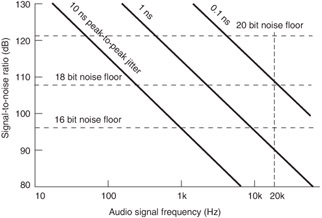
Figure 6.7: Effects of sample clock jitter on signal-to-noise ratio at different frequencies, compared with theoretical noise floors of systems with different resolutions. (After W. T. Shelton, with permission.)
When jitter is periodic rather than random, it results in the equivalent of 'flutter', and the effect when applied to the sample clock in the conversion of a sinusoidal audio signal is to produce sidebands on either side of the original audio signal due to phase modulation, whose spacing is equal to the jitter frequency. Julian Dunn 4 has shown that the level of the jitter sideband ( R j ) with relation to the signal is given by:
R j (dB) = 20 log ( J ‰ i /4)
where J is the peak-to-peak amplitude of the jitter and ‰ i is the audio signal frequency. Using this formula he shows that for sinusoidal jitter with an amplitude of 500 ps, a maximum level 20 kHz audio signal will produce sidebands at -96.1 dB relative to the amplitude of the tone.
What is important, though, is the audibility of jitter-induced products and Dunn 4 , 5 attempted to calculate this based on an analysis of the resulting spectrum using accepted audibility curves, based on critical band masking theory, assuming that the audio signal is replayed at a high listening level (120 dB SPL). As shown in Figure 6.8, which plots jitter amplitude against jitter frequency (not audio frequency) for just-audible modulation noise on a worst-case audio signal, the jitter amplitude may in fact be very high (>1 s) at low jitter frequencies (up to around 250 Hz) because the sidebands will be masked at all audio frequencies, but the amount allowed falls sharply above this jitter frequency although it may still be up to 10 ns at jitter frequencies up to 400 Hz.
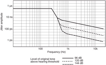
Figure 6.8: Sample clock jitter amplitude at different frequencies required for just-audible modulation noise on a worst-case audio signal. (After J. Dunn, with permission.)
The original version of AES11 specified tolerances for jitter on the sampling frequency clock, but this was dropped in the 1997 revision in favour of a statement to the effect that the clock tolerance requirements for A/D and D/A conversion would have to be more stringent than that for a Grade 1 reference signal in respect of random jitter and jitter modulation. This reinforces the point that sampling clock jitter and interface clock jitter are related but different problems. The effect of jitter on sampling clocks and the audible result thereof has become a large and complex subject and it is not proposed to deal with it further in this book, the primary purpose of which is to cover interfacing issues. A comprehensive study by Chris Dunn and Malcolm Hawksford 6 attempted to survey the effects of interface-induced jitter on different types of DAC and this paper warrants close study by those whose business it is to design high quality DACs with digital audio interfaces.
The implication of section 6.4.1 is that it is greatly preferable to derive a stable sample clock from one of the reliable preamble transitions than from the audio data slot transitions, although there is evidence that many devices do use the data transitions. One older interface receiver chip adjusted its PLL on every negative-going transition in the interface signal, for example. Since transitions in the audio data part of the subframe are not only more sensitive to line-induced jitter, but also determined by the audio signal, it is even possible for a signal on the B audio channel to modulate the sampling clock such that jitter sidebands appear in the A channel that are tonally related to the signal in the B channel.
The rejection of jitter by the receiver depends principally on the frequency response of its PLL and in general the narrower the response of the PLL and the lower its cut-off frequency the better the rejection of jitter. The problem with this is that such PLLs may not lock up as quickly as wide bandwidth PLLs and may not lock over a particularly wide frequency range. A solution suggested by Dunn and Hawksford is to use a wideband PLL in series with a low bandwidth version which switches in after conditions have stabilized. Alternatively RAM buffering may be used between the interface decoder and the convertor, the data being clocked out of the buffer to the convertor under control of a more stable clock source. In a hi-fi system it is possible that the stable clock source's frequency could be independent of the incoming data clock, provided that the buffer was of sufficient size to accommodate the maximum timing error between the two over the duration of, say, a CD, but the better solution adopted by some manufacturers in two-box CD players is to generate a synchronizing clock in the convertor which is fed back to reference the speed of the CD transport and thus the rate of data coming over the digital interface (see Figure 6.9).
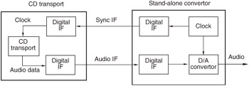
Figure 6.9: In one high quality CD player with a separate convertor, rather than deriving the convertor clock from the incoming audio data, the convertor clock is fed back to the transport via a separate interface in order to maintain synchronization of the incoming data.
In a professional digital audio system where all devices in the system are to be locked to a common sampling frequency clock it would normally be necessary to lock any convertors to an external reference. An AES11-style reference signal derived from a central generator might have suffered similar degradations to an audio signal travelling between two devices and thus exhibit transition timing jitter. In such cases, especially in areas where high quality D/A conversion is required, it is advisable either to reclock the reference signal or to use a local high quality reference generator, slaved to the central AES11 generator, with which to clock the convertors.
| | ||
| | ||
| | ||
EAN: 2147483647
Pages: 120