4.4 Modern Physical Design Techniques
In the age of deep submicron design, where 10+ million gates of logic have to fit on a single device running at 250+ MHz, traditional physical-design techniques are not capable of handling these new challenges. The problems with the traditional physical-design techniques can be summarized as follows :
-
Timing closure is either unachievable or takes too long to finish.
-
Too many iterations between front end and back end for each design.
-
Unroutable designs for the target die size .
As the device geometries shrink to 0.11 micron and beyond, new tools, techniques, and methodologies are needed to overcome the problems we face with traditional approaches.
Here in this section, we cover two examples of modern physical-design techniques. The new methods presented here both overcome the above challenges and substantially simplify the physical design.
The Silicon Virtual Prototype [1]
[1] Courtesy of Silicon Perspective, Inc. (A Cadence Company). Portions reprinted with permission.
In the mid-1990s, two important issues were converging to make physical chip designers' lives miserable. First, they were being asked to put more and more on a single chip. The integration challenge really hit home as chip design approached the million-gate hurdle and physical-design tools choked on the complexity. Second, the interconnect started to have a much stronger effect on the timing for the entire chip. Timing closure became a huge issue because most physical-design tools did not comprehend the effects of the interconnect.
As a result of these two issues, chip physical implementation became a huge problem, especially as geometries shrank to 0.25 microns and below. Logic designers were told that their designs simply couldn't meet timing. Physical designers were dismayed at the lengthy run times of their choking tools, especially when many iterations were required to converge on a physical implementation that could meet all the timing, area, and power requirements.
The existing methodology promoted an arm's-length working relationship between the front-end logic-design team and the back-end physical-layout team. Each group used completely different tools, geared specifically for its use only. This methodology relied on multiple iterations between the front and the back ends. As a result, new chip designs were significantly delayed.
What did designers do? There seemed to be two choices. One was to resort to overly pessimistic designs with wider than necessary guardband as a safety margin. However, this flew in the face of the demands for higher and higher performance. The other choice was to suffer the pain of 20 or more iterations between synthesis and layout, if they ever brought about a timing closure at all.
What was needed was a tool/methodology combination that effectively bridged the gap between the front-end logic design and the back end, where the tools were falling far short. This new technique needed to provide fast turnaround for quick feedback between the front end and back end instead of the days or weeks required to complete one layout iteration and generate the necessary timing and simulation data for feedback to the front-end process. What also was needed was a totally new approach that squeezed between the front end and back end. That new approach is what is now called the silicon virtual prototype, and is what has made it possible to design multimillion-gate chips today.
This section will discuss how First Encounter from Cadence's Silicon Perspective subsidiary can be used to create a silicon virtual prototype, helping designers to reduce iterations and finish large-chip designs much faster.
Silicon Virtual Prototyping
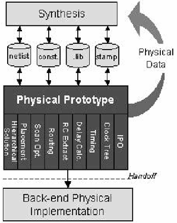
The silicon virtual prototype is the practical approach to dealing with increased complexity and the challenges of timing closure with deep submicron (DSM) silicon. The silicon virtual prototype creation is the first stage of the back-end design phase, often before all of the front-end design is complete. By creating a full-chip silicon virtual prototype, the design team can immediately validate the physical feasibility of the netlist ”eliminating the back-end design iterations that were required to discover that a chip could not meet timing or some other constraint. Figure 4.9 illustrates the environment for physical prototyping.
Figure 4.9. Physical Prototype Environment
The silicon virtual-prototyping stage compresses the physical-feasibility stage down to a few hours so chip designers can view the chip layout once or more each day. Now designers can evaluate many implementations of their designs and get quick feedback on the best trade-offs. Key to the speed is the revolutionary change in tool-database architectures. Design files for traditional tools tended to be very large, limiting the maximum design size they could effectively handle. The new tools employ lightweight databases that let them handle multimillion-gate designs with ease.
The creation of the prototype also allows the designers to create realistic timing budgets for all sections of the chip. These timing budgets can be set based on real physical information from the actual design rather than an estimate.
The New Design Flow
In this new methodology, designers may start building their silicon virtual prototype at a very early stage in a chip's development process. For a very large design, the prototype creation can begin when portions of the design are incomplete. Black boxes can be used to estimate those regions that are not complete or consist of third-party IP.
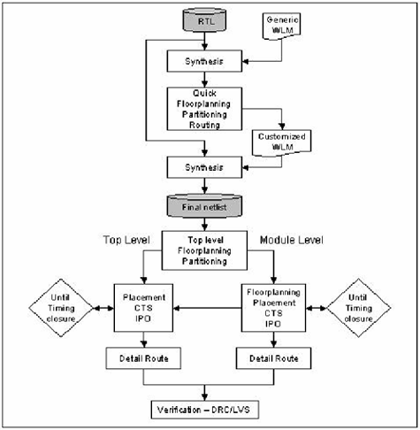
Figure 4.10 shows the design flow for silicon virtual prototyping. Once the functionality of the chip is fully defined, the first step in this methodology is to perform a quick logic synthesis to create a gate-level netlist. It is assumed that the netlist is functionally clean but that timing is not accurate, so simple wire-load models (WLMs) can be used at this stage. The resulting gate-level netlist plus the timing constraints form the inputs to the creation of the silicon virtual prototype.
Figure 4.10. Design Flow for Silicon Virtual Prototyping
The creation of the silicon virtual prototype begins with fundamental full-chip floorplanning activities such as I/O placement, macro placement, and power topology. Major design elements usually are manually placed based on the designer's knowledge of the chip architecture. The remaining elements can be automatically placed for maximum efficiency.
Conventional floorplanning tools start by creating block shapes and fitting them together, then use this template to try to drive a full layout. Floorplanning for a silicon virtual prototype works in almost exactly the opposite way. It creates a full, flat placement of all standard cells and macros for the entire chip. Silicon Perspective's First Encounter tool uses an algorithm (called Amoeba ) to generate a fast placement that is timing driven and intelligently blends logical hierarchy and physical locality to optimize concurrently for timing, power, die size, and routability. The Amoeba clustering technology preserves the logic hierarchy on the physical side so changes can be traced through the design.
For the first pass at floorplanning, a netlist, physical libraries, corresponding synthesis libraries (.lib), top-level constraints, and a technology file (process description) are created and imported. This data can be automatically loaded for succeeding passes . Specific macro and I/O placements can be established and then saved into a command file so they can be read in for later iterations. Placement guidelines can be generated and saved to indicate , for example, that certain cells need to be placed close to the I/Os. Placement guides usually are created for the major modules and used to guide the placement engine as where to roughly place the module cells. A script for power/ground topology also can be created.
Next , the remaining standard cells are placed using a timing-driven algorithm. The placement includes a trial route that ensures that major congestion issues are eliminated. The design is then extracted and the timing analyzed . This gives the design team a quick idea of the physical feasibility of their design and allows them to experiment with different placements to determine the most desirable aspect ratio and optimum block locations.
Timing Closure
Conventional approaches to timing-driven layout typically rely on slack -based, constraints-driven algorithms. These are "explicit" timing-driven methods in that they depend on prespecified timing constraints to direct the layout operation. These techniques work relatively well when the design is small, but with any design of reasonable complexity, the algorithms bog down and performance deteriorates rapidly . In addition to being very hard to use and slow to run, these conventional approaches often achieve timing closure at the expense of layout quality in the areas of wire length, die size, and routability.
In contrast, the Amoeba placement engine takes an "implicit" approach to timing control. Throughout the entire floorplanning and placement process, it tries to exploit the natural clustering characteristic that is intrinsic in a design's logical hierarchy. Instead of depending on externally imposed constraints, the Amoeba engine naturally blends logical hierarchy and physical locality in its core algorithmic foundation. By exploiting the logical hierarchy, physical locality is achieved naturally, in tandem with optimizing wire length, timing performance, chip die size, and layout routability.
The Amoeba engine applies this hierarchical-locality-based approach to a unified floorplanning and placement task. At any given level of a typical hierarchical chip design, intramodule signals account for over 95 percent of all signal nets , leaving fewer than five percent for intermodule signals. The physical locality implicitly leads to shorter wire lengths for intramodule signals, which generally require smaller drivers. Exploiting this characteristic allows the Amoeba technology to focus on the intermodule signals, which are greatly reduced in number and tend to be more critical. The Amoeba engine applies techniques such as net weighing, soft and hard planning guides, grouping/regrouping, and rehierarchy. Additionally, hard placement fences are employed, interwoven with other features such as power/ground strips and obstructions.
The Amoeba technology only needs to deal with a very drastically reduced number of signal paths at any given stage in the placement process because it applies the physical locality and intramodule/intermodule signal distribution hierarchically and incrementally. This greatly enhances its speed and allows it to more thoroughly explore the possible solution space to develop an optimum solution considering all the factors of timing, area, and power consumption.
The Amoeba technology uses an intelligent-fencing strategy to place circuit cells. Conventional placement approaches confine cells in a design module to a nonoverlapping "fenced" rectangular or rectilinear area. Such rigidity leads to wasted die area and greatly impaired routability. With the intelligent -fencing strategy, Amoeba allows two clusters to overlap when and if necessary, leading to more efficient die usage, shorter wire lengths, and much better routability.
One of the big benefits of the Amoeba-based approach is that it helps designers make intelligent decisions about allocating timing budgets among different blocks. Designers can easily see if certain parts of the chip are overconstrained or underconstrained and make the appropriate adjustments. Here, the budgets are set based on real physical data.
To verify timing closure, designers compare the timing data produced by the prototype against the final tape-out version of the chip. By comparing the Standard Delay Format (SDF) files produced by an extraction and timing analysis of both versions of the design, the design team can make sure timing goals are met. Correlation results for this type of analysis should yield 90 percent of the nets to be within 10 percent.
Design Partitioning and Hierarchical Techniques
This new methodology mixes the best of both hierarchical and flat design. By first creating a totally flat global view of the entire design and evaluating different physical placement options (in the step described above), designers get the best of flat design techniques. However, most tools choke on multimillion-gate flat designs. Therefore, a top-level partitioning can be employed to optimally break the chip into a number of hierarchical blocks for physical implementation. The hierarchical approach also makes it possible to have multiple design teams working in parallel on different sections of the chip, speeding the completion of the design.
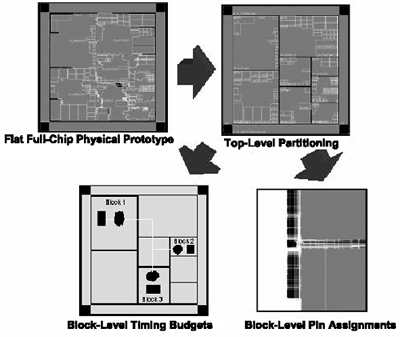
Hierarchical methodologies have been widely adopted in the front-end logical design world. However, designers have hesitated to embrace hierarchical methodologies for physical design because of the challenge of generating accurate timing budgets and pin placements for the blocks. First Encounter provides the intelligence designers need to allocate timing budgets among the blocks and to determine optimal pin placements. Figure 4.11 shows how the full-chip physical prototyping drives partitioning.
Figure 4.11. The Full-Chip Physical Prototype Drives the Partitioning
The silicon virtual prototype is the starting point for creating a physical hierarchy in the design. During the import, all modules are flattened to create the prototype. The standard cells are placed flat at the top; the design is then routed and extracted and the timing is analyzed. This is when the partitioning is implemented to re-create the hierarchy.
The tool creates a directory of data for each partition, including the top level. Each directory contains a netlist, floorplan file, pin assignments, and timing constraints. In addition, the subdirectory for the top cell contains a block view for each partition.
Reaching the optimal block size in large designs often requires two levels of partitioning. The size of these sub-blocks is driven by the capacity of the tools, such as physical synthesis, that seem to perform best on blocks of 100,000 gates. For example, a design of five million gates would be partitioned into 10 blocks of 500,000 gates. Those blocks would then be partitioned into sub-blocks of approximately 100,000 gates.
To be able to perform the second-level partitioning, the constraints that were created as a result of the partitioning must be combined with the multicycle and false- path constraints for each partition. As with the major partitions, placement, routing, extraction, and timing analysis will derive the necessary timing budgets for the second-level partitions, which then can be passed to a physical-synthesis tool.
Automatic Pin Assignment
First Encounter can produce an automatic, optimized assignment of pin locations on chip partitions, using both detailed logical and physical information. This eliminates a time-consuming , tedious , and error-prone task.
Block-Level Physical Synthesis, Place, and Route
Physical synthesis tools can be used on each block of the hierarchical design. Additionally, block-level place-and-route tools, such as Cadence Silicon Ensemble-PKS or Synopsys' Physical Compiler, are used at the block level. As each block is completed, it is placed back into the silicon virtual prototype to make sure the design is on target for timing, area, and power.
Chip-Level Implementation for Hierarchical Design
As the design team creates the physical blocks, they are assembled back into the silicon virtual prototype. However, a number of top-level or chip-level tasks are also required. The master clock network for the chip must be generated, the power and ground framework must be designed, and the top-level interconnect and buffering must be created. First Encounter provides advanced capabilities that supplement the design team's existing router for these tasks .
A key element of chip-level assembly is managing buffers between the design's partitions in order to achieve top-level timing closure. First Encounter works with popular commercial routers to provide a fast, flexible mechanism based on either rules or timing. First Encounter performs top-level buffer insertion when the prototype is created. However, in practical design flows, minor netlist changes continue to be made within the chip's blocks well into the physical design stage; often these changes have implications for top-level chip timing and even routing.
In-place optimization (IPO) downsizes, upsizes, and inserts buffers and repeaters to obtain an optimal timing once all the block designs are complete. IPO needs to be performed at the top level to guarantee timing closure at the partition boundaries.
The next step is clock-tree synthesis. First Encounter's clock-tree synthesis option creates a complete clock tree at both the top level and the block level, leveraging the Amoeba-placement algorithm to minimize skew and insertion delay. Even very complex clock structures can be handled.
In hierarchical design flows, most design teams use automated tools to generate clock structures within the chip's partitions. However, top-level clock trees usually are created manually. First Encounter's clock-tree synthesis provides automation at both levels, leveraging the Amoeba ultra -fast placement technology to generate and optimize a top-level buffer-tree network that balances the clock-phase delay for minimum skew between the chip's partitions. This results in major time savings over manual methods.
First Encounter's clock-tree synthesis supports gated clocks for use in power-sensitive applications and generates a clock-routing guide for final detailed routing.
Power Grid Design
Power distribution has become a significant concern in SOC designs. Most designers now routinely over-design their chip power grids in order to prevent IR-drop problems. However, not only does this interfere with signal routing (congestion), but it also increasingly does not guarantee that IR-drop violations will be avoided.
The First Encounter Power Grid Designer option addresses this problem. It enables designers to lay out and analyze the chip's power and ground network early in the physical design cycle, with accurate correlation to the final layout. This detects potential IR-drop problems early in physical design, instead of at the end of the layout cycle. Power Grid Designer leverages First Encounter's trial route, extraction, and delay calculation engines to deliver results that previously required an entire physical layout cycle to achieve. This, in turn , allows designers to optimize the power grid while the cost of correcting problems is still low.
Benefits of the Silicon Virtual Prototype
One of the key benefits of developing a silicon virtual prototype is the turnaround speed of each iteration. In a traditional design flow, information about physical feasibility is available only after the completion of place and route followed by final verification. This process typically takes several days. A silicon virtual prototype tool must be able to validate the physical feasibility of a large SOC design in a few hours on a desktop workstation.
There are numerous other benefits as well. The silicon virtual prototype provides a vehicle for much better and increased communication between the front-end designers and the back-end designers. Design teams can try new approaches and quickly find out if they're on the right track or if they are wasting their time. Above all, the silicon virtual prototype provides an efficient way to speed designs through the physical design cycle. First Encounter provides a production-ready placement that is ready for final routing.
New Approach for Implementing Big IC Design [2]
[2] Courtesy of AmmoCore Technology, Inc. Portions reprinted with permission.
Shrinking device size is driving increased gate count in ICs, but the design methodology is not keeping up with the pace. Most design houses have EDA tools and hardware that can run flat designs up to two million gates or hierarchical designs up to four million gates. Most of the hierarchical design methodology uses block-based design, with each block size averaging 200,000 to 500,000 gates.
There are no alternatives to designs over two million gates, but block-based designs have several rigid constraints both in terms of timing as well as physical real estate in a given die.
Block-Based Design
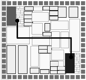
As shown in Figure 4.12, the block-based design methodology imposes artificial boundary constraints. It is very difficult to meet the critical timing path requirements. While it is easier to meet the block-level timing constraints, it is very difficult to meet chip-level timing requirements. This causes endless iterations to close chip-level timing requirements. In most cases, the chip speed is sacrificed to meet the market window.
Figure 4.12. Block-Based Design
Several EDA vendors have come up with floorplanning solutions, hoping to solve the mysteries of timing closure, but they all failed because early gross estimation is as good as no estimation.
The challenge is how to arrive at a 98 percent confidence level within a few hours, not in a few days. Achieving even 70 percent is not good enough, which is the claim of most floorplan vendors.
New Approach
The new approach, as shown in Figure 4.13, is to break down these rigid boundaries of physical blocks and come up with faster, more fluid solutions. Ammocore Technology, Inc., has come up with a unique approach that allows designers to minimize their floor-planning task, break their design into smaller groups, and process all these groups via parallel processes. This methodology allows designers to gather meaningful data within a few hours without hitting any design size (gate count) limitations, and it offers proof that a design of four million gates can be implemented within 14 hours from netlist to GDSII.
Figure 4.13. New Approach to Physical Design
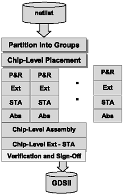
Design Flow
There are five major steps in the implementation for this new approach. The steps are floorplanning, partitioning, placement, assembly, and verification. Figure 4.14 shows the design flow for this new approach.
Figure 4.14. Design Flow
Floorplanning
In this basic floorplanning step, designers place the hard macros (e.g., RAM, ROM, IP core) and implement power for such macros. There are no requirements for doing month-long floorplan optimizations based on wire-load models. Typically, this can be done within an hour for a large design.
Partitioning
The partitioning step not only considers connectivity and timing but also looks at the available spaces in the die. This step breaks the design into manageable pieces and is the key to meet timing and routing requirements in fewer iterations. All these pieces are then implemented using parallel processing, before proceeding with the top-level placement.
Placement
Placing all the partitioned pieces at the chip level provides significant insight into the likelihood of meeting both timing and routing requirements. If there are issues in timing or routing, designers can fix them by inserting buffers or optimizing logic, or even by programming minor perturbation of the placement. The time it takes to do partitioning and placement is about an hour for a design of up to four million gates.
Assembly
Assembly happens in two steps, first on the small pieces and then on the chip level. Assembly time is significantly reduced due to the nature of two-step process: Designers can debug any timing issues related to critical paths faster by using these two steps. As a result, the router needs to evaluate a smaller percentage of nets at the top level.
Verification
Verifying a large design is always tricky. Many design houses struggle to come up with a streamlined process for timing and physical verification before submitting the design to the mask shop. Our approach is to divide the problem into a more manageable size and then process the pieces in a massive parallel fashion. In this way, most of the issues will be resolved before the design is sent for a final verification using traditional tools that takes days, if not weeks.
In summary, traditionally, block-based design methodology is used for large designs, but it imposes many constraints on a designer. Block-based methodology requires several iterations at the block level as well as at the chip level. In many cases, it is very difficult to achieve the performance goals due to the nature of rigid boundaries in the die.
The new approach breaks these boundaries and provides an innovative way to handle design of any gate count. Managing the data and processing it in a massively parallel way reduce debugging time to a ratio of 1:100. The two-step process also improves the design implementation time to a ratio of 1:10.
| |
| Top |
EAN: 2147483647
Pages: 61
- Chapter III Two Models of Online Patronage: Why Do Consumers Shop on the Internet?
- Chapter VIII Personalization Systems and Their Deployment as Web Site Interface Design Decisions
- Chapter IX Extrinsic Plus Intrinsic Human Factors Influencing the Web Usage
- Chapter XII Web Design and E-Commerce
- Chapter XIII Shopping Agent Web Sites: A Comparative Shopping Environment