Differential Timing Characteristics
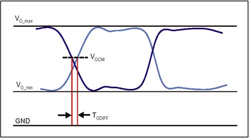
| This section defines the timing parameters for CAD[n:0], CTL, and CLK[m:0]. The HyperTransport link uses a simple timing methodology that accounts for simultaneous worst case combinations of uncertainties. This timing methodology attempts to cover all cases that could occur in operational systems, and is defined to provide zero additional margin. This means that board designers and designers of device transmitter and receiver interfaces must meet specification requirements over all process, voltage, and temperature corner cases. Differential Signal SkewThe maximum skew allowed by the output driver between the true signal and its differential complement is defined as T ODIFF. Figure 14-10 on page 380 illustrates this parameter, which is measured at the mid-point of the transition of the differential signal with respect to ground (i.e., the common-mode point). The maximum skew allowed is limited by Delta-V OCM being within specification. Figure 14-10. Output Skew Measurement T IDIFF is also defined by the specification, which is the maximum skew allowed at the input of the receiver. Specifically, T IDIFF defines the max skew allowed between the true signal and its differential complement measured at the mid-point of the transition of the signal which is input to a receiver. The measurement for T IDIFF is made in the same manner as for T ODIFF. Table 14-11 on page 380 lists maximum skew permitted at the output of the driver and for the input of the receiver at various transmission rates. Table 14-11. Maximum Differential Output and Input Skew Values
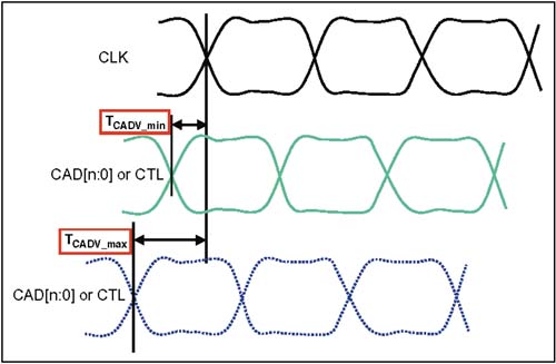
Source Synchronous Clock SkewThe source synchronous clocking employed by HT requires that CLKOUT be delayed by one-half bit time to align the clock edge in the center of the CADOUT and CTLOUT bit time. This represents a 90 degree phase shift on clock relative to the CADOUT and CTLOUT signals. Similarly, the specification defines the maximum skew permitted at the receiver between CLKIN and CADIN or CTLIN. The specification permits some tolerance in the clock delay relative to CAD and CTL for both the driver output and receiver input. Source Synchronous Clock Skew at the TransmitterThe specified parameter for the output measurement is called CAD valid time (T CADV ). Figure 14-11 on page 382 illustrates the relationship between CLKOUT and CADOUT or CTLOUT. An example of this relationship is discussed below: Figure 14-11. T CADV Minimum and Maximum Measurements Assuming an 800MHz clock (which yields 1600MT/s), the clock period is 1250ps, and the bit-time period (TBIT) is 625ps. When CADOUT[n:0] or CTLOUT is driven, the CLKOUT signals should be driven one-half bit time later (TCADV_typical = 312.5ps). The margin of skew allowed between CLKOUT and CADOUT[n:0] or CTLOUT is a function of the uncertainties related to the transmitter PHY, transmitter package skew, and transmitter clock. The minimum and maximum values are defined below:
Table 14-12 on page 382 lists the permitted values for T CADV. Table 14-12. Source Synchronous CLK Output Skew Values
Source Synchronous Clock Skew at the ReceiverAt the receiver end, source synchronous clock skew is affected by motherboard PCB skew. The PCB CLK trace length and median of the associated CAD/CLK length must be matched so that setup and hold time for CAD/CLK signals are not violated at the receiver. Realistically, the specification allows for some motherboard skew between CAD/CTL and its associated CLK signal. Two factors contribute to this skew:
The source synchronous clock skew parameter at the receiver is termed CAD valid time at receiver (T CADVRS ).
T CADVRS and T CADVRH are measured at the receiver over a large number of samples and conditions which maximizes PCB skew. Table 14-13 on page 383 lists the minimum and maximum skew values. Table 14-13. Source Synchronous CLK Input Skew Values
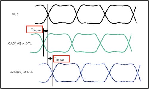
Setup and Hold TimingFigure 14-12 on page 384 illustrates the setup and hold timing parameters and Table 14-14 on page 385 specifies the values at different transmission rates. The parameters are defined as follows :
Figure 14-12. Setup and Hold Time for CAD and Control Table 14-14. Setup and Hold Times for CAD and CTL
|
EAN: 2147483647
Pages: 182