3.1 Motherboard Characteristics Several characteristics differentiate motherboards, including physical characteristics, which in combination are called the form factor; the chipset used, which defines the capabilities of the motherboard; the processors the motherboard supports; the BIOS it uses; and the internal and expansion buses that it supports. The following sections examine each of these factors. 3.1.1 Form Factor Motherboards differ in size, shape, position of mounting holes, power supply connector type, and port types and locations. Together, these differences define the form factor of the motherboard. Form factor is a critical issue when you upgrade a system, because the replacement motherboard must physically fit the case and use the existing power supply connectors. Form factor doesn't matter when you're building a new PC. You simply select the best motherboard for your needs, and then buy a case that fits it. Many motherboard manufacturers build similar motherboards in different form factors. Here are the form factors you may encounter: - AT, Baby AT (BAT), and LPX
-
All of these form factors are based on the motherboard used in the original 1984 IBM PC AT and are now obsolescent or, in the case of LPX, obsolete. Although it is still possible to buy AT and BAT motherboards, selection is limited (e.g., Athlon and Pentium 4 motherboards are not available in these form factors) and most AT and BAT motherboards do not include the latest chipsets and other technologies. The only reason to buy an AT or BAT motherboard is to upgrade an existing system without replacing the power supply and case. Good cases with power supply are available for $65 or so, and the power supply in an older case is likely to be near the end of its life, so we do not recommend buying a motherboard in any of these form factors. - ATX and variants
-
Nearly all current motherboards use the ATX form factor, or one of its smaller variants, the miniATX,  ATX, FlexATX, and NLX. For a complete discussion of these form factors, including case and power supply issues, see Chapter 25 and Chapter 26. ATX, FlexATX, and NLX. For a complete discussion of these form factors, including case and power supply issues, see Chapter 25 and Chapter 26. - Proprietary
-
Although it is much less common nowadays to find new systems that use proprietary motherboards, such boards were relatively common a few years ago, particularly in systems sold by major manufacturers like Compaq and IBM. A cynical observer might believe that the major manufacturers did this to lock customers in. In fact, it probably had more to do with the fact that the then-current Baby AT standard had reached the end of its useful life and the ATX standard had not yet become the obvious successor. To reduce manufacturing costs and increase reliability, manufacturers that had the in-house engineering talent to do so designed their own motherboards. Some of these are actually very elegantly designed. They all share one fatal flaw, however: they aren't standard. Any system that uses a proprietary motherboard form factor is effectively not upgradable. 3.1.2 Chipsets Just as the motherboard defines a PC, the chipset defines a motherboard. The chipset determines the main characteristics of the motherboard what processors it supports, what RAM types it can use, what bus types and speeds it supports, whether it supports standards like AGP and USB, and so on. Chipsets are so named because they usually comprise two relatively large chips. Some chipsets contain three or more chips. A few chipsets, most of which are intended for low-cost systems, have all functions on one physical chip. Figure 3-1 shows a block diagram for the 815E, Intel's flagship chipset for the Pentium III and Celeron processors. Block diagrams are helpful in understanding the functions of a chipset. Like most chipsets, the 815E comprises a Northbridge chip, labeled GMCH, and a Southbridge chip, labeled ICH2. The Northbridge interfaces the CPU, memory, and AGP video all high-bandwidth components. The Southbridge can conveniently be thought of as a peripheral controller. The Southbridge manages low- and moderate-bandwidth components such as the PCI bus, IDE interface, USB ports, and so on. Some motherboards supplement Southbridge functions by adding another chip, often called a Super I/O controller. Figure 3-1. Block diagram of the Intel 815E chipset (graphic courtesy of Intel Corporation) 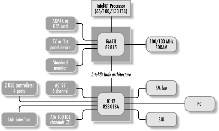 Chipset makers often use one Southbridge with different Northbridges to create chipsets for different processors. For example, Intel uses the 82801BA ICH2 Southbridge in numerous chipsets, some of which support the Pentium III and Celeron, and others the Pentium 4. It's also possible to use the same Southbridge to create chipsets for processors from different makers. For example, VIA Technologies produces chipsets for the Intel Pentium 4 and AMD Athlon two processors with very different architectures by combining the same Southbridge with a Northbridge that supports the processor in question. There are scores of motherboard manufacturers, but only a handful of chipset manufacturers. This is because designing a chipset requires significant engineering resources, but building a motherboard around that chipset is straightforward. Chipset manufacturers want motherboard manufacturers to buy their chipsets, so they provide detailed specifications and engineering drawings, which makes building motherboards more a matter of production than design. If you examine twenty motherboards made by twenty different manufacturers, all using the same chipset, you'll find that the similarities outweigh the differences. There may be minor variations in features and layout, but the chief differences are the quality of the components used and the quality of construction. Accordingly, it is quite possible for one manufacturer to make a terrible motherboard and another manufacturer a superb motherboard, even though both use the same chipset. The motherboard market is so competitive that price is almost invariably an excellent predictor of the quality of a motherboard. Understanding chipset basics is important whether you are upgrading an existing PC or building a new one. If you are upgrading, understanding the chipset tells you what can and cannot be done within its limitations. It also helps you avoid useless or counterproductive upgrades. For example, the Intel 430TX Pentium chipset supports 256 MB RAM but caches only 64 MB, so adding more than 64 MB to a 430TX system can actually reduce performance. If you are building or buying a new PC, its chipset is the most important factor in determining motherboard performance and future upgradability. Understanding the differences between competing chipsets lets you make rational decisions about which computer or motherboard to buy. Because chipsets are so important, we've devoted a great deal of space to explain what you need to know about chipsets. 3.1.2.1 CPU Family Support Chipsets support only one of these CPU families: - Intel 486 and similar fourth-generation CPUs
- Intel Pentium and compatible fifth-generation CPUs
- Intel Pentium Pro/Pentium II/Celeron/Pentium III sixth-generation CPUs
- Intel Pentium 4 seventh-generation CPUs
- AMD Athlon/Duron sixth-generation CPUs
This is because processor families differ greatly in how they access and manage main memory, cache, and other major system components. For example, while fifth-generation CPUs use separate L2 cache memory on the motherboard, sixth-generation CPUs have L2 cache within the processor package or integrated on-die. A particular chipset may support most or all CPUs within a family, or may support only one of them. For example, some chipsets support the Pentium II, Celeron, and Pentium III CPUs, while others support only one or two of those. Most chipsets designed for the Pentium also support compatible processors like the AMD K5 and K6 and the Cyrix 6x86 and 6x86MX, which were designed as pin-compatible, although using one of these CPUs may require different motherboard jumper settings and chipset CMOS parameters than those used for a genuine Pentium. Also, chipsets designed for late variants within a generation may not support earlier variants within that generation. For example, Intel 815-family chipsets do not support the Pentium II and early variants of the Celeron. There is also the issue of hybrid processors, which straddle generations. For example, recent Pentium-compatible CPUs like the AMD K6-2/III and the Cyrix 6x86MX have sixth-generation features that are not supported by older chipsets, particularly Intel chipsets. These processors are sixth-generation internally, or largely so, but physically fit fifth-generation motherboards. To encourage migration to the Pentium II, Intel stopped developing fifth-generation chipsets. Third-party chipset manufacturers, notably VIA, SiS, and ALi, took up the slack by introducing enhanced fifth-generation chipsets called Super Socket 7 chipsets. Using these chipsets allowed manufacturers to build motherboards that supported features not supported by Intel fifth-generation chipsets, such as AGP. 3.1.2.2 CPU Speed Support A chipset that supports a particular CPU may support all or only some of the speeds that that CPU is available in. In general, faster CPUs require faster chipsets, so you might imagine that a chipset rated to handle the fastest version of a particular CPU could also handle all slower versions of that CPU. That's not always the case, however. Modern motherboards accommodate different processor speeds by varying two settings, memory bus speed and CPU multiplier. - Memory bus speed
-
This is the speed at which the CPU communicates with system memory. Intel Pentium-class chipsets support Intel's official memory bus speeds of 50 MHz, 60 MHz, and 66 MHz. Third-party chipsets also support these standard speeds, and may also support other speeds, including 75 MHz, 83 MHz, 90 MHz, 95 MHz, 100 MHz, and 112 MHz. All sixth-generation chipsets support a 66 MHz memory bus speed, which is called front-side bus (FSB) speed on sixth-generation systems. Later versions may also support 100 MHz and 133 MHz, along with various intermediate speeds. Early Athlon motherboards supported only the 100 MHz FSB (although it is "double-pumped" and so referred to as 200 MHz). Later Athlon motherboards also support the 133/266 MHz FSB, and the latest also support the 166/333 MHz FSB. For many motherboards, including most Intel motherboards and third-party motherboards, setting the memory bus speed also specifies the PCI bus speed. These motherboards, called synchronous motherboards, divide the memory bus speed by a fixed factor to determine PCI bus speed. For 50 MHz, 60 MHz, and 66 MHz memory bus speeds, the divisor is 2.0, which runs the PCI bus at 25 MHz, 30 MHz, and 33 MHz, respectively. For a 100 MHz bus, the divisor is 3.0, which runs the PCI bus at 33.3 MHz. For 133 MHz, the divisor is 4.0, which also runs the PCI bus at 33.3 MHz. Some motherboards, called asynchronous motherboards, allow memory bus speed and PCI bus speed to be set independently, usually by means of jumpers on the motherboard. They do this to allow using faster memory bus speeds while limiting PCI bus speeds to 33 MHz, which is the fastest reliable setting for the PCI bus. Otherwise, for example, with a processor designed to use a 100 MHz FSB, setting the memory bus to 133 MHz would run the PCI bus at 44.4 MHz (one third of 133), which is much too fast for reliability. - CPU multiplier
-
This specifies the multiple of memory bus speed at which the CPU runs internally. Modern chipsets may support CPU multipliers from 1.5x to 10.0x or higher. For example, a 90 MHz Pentium CPU uses a 60 MHz memory bus speed and a 1.5x CPU multiplier, while a 1.2 GHz Pentium III uses a 133 MHz memory bus speed and a 9.0x CPU multiplier. All recent AMD and Intel CPUs have a locked multiplier, which means the only way to run them faster than their rated speed is to set the FSB for something above nominal. For example, setting the FSB to 150 MHz rather than the nominal 133 MHz for a 1.2 GHz Pentium III runs the CPU at 1350 MHz (150 x 9.0). That results in a small performance increase, but also reduces system stability, because the PCI bus is running at 37.5 MHz (150/4) rather than its design speed of 33.3 MHz. On fifth-generation and early sixth-generation motherboards, you can generally determine the range of CPU speeds supported by a chipset and motherboard by examining the different memory bus speeds and CPU multipliers that it supports. For example, a typical Pentium motherboard may provide nominal memory bus speeds of 50, 60, and 66 MHz (actually, 50.0, 60.0, and 66.6 MHz), and CPU multipliers of 1.0, 1.5, 2.0, 2.5, and 3.0x. This motherboard will support Pentiums running at 75 MHz (50 x 1.5); 90 MHz (60 x 1.5); 100 MHz (66 x 1.5); 120 MHz (60 x 2.0); 133 MHz (66 x 2.0); 150 MHz (60 x 2.5); 166 MHz (66 x 2.5); and 200 MHz (66 x 3.0). The motherboard could also be configured for speeds e.g., 180 MHz (60 x 3.0x) for which no processors are available. You may also have a choice of two or more speed/multiplier combinations to use. For example, you could install a 100 MHz CPU on this system board using either 66 MHz with a 1.5 multiplier or 50 MHz with a 2.0 multiplier. Generally, use the combination that uses the fastest memory bus speed, which provides faster performance. However, sometimes it makes sense to choose a slower memory bus speed. For example, you may install a 450 MHz CPU and memory that is allegedly rated for 100 MHz, but find that the system is unreliable using 100 MHz and 4.5x. Changing to 90 MHz and 5.0x runs the processor at the same speed, but the memory at only 90 MHz rather than 100 MHz, which may allow the system to run reliably with only a small performance hit due to the slower memory speed. Not all motherboards allow these two parameters to be set independently. Many motherboards, including early sixth-generation Intel models, allow you to set only CPU speed, which in turn selects a predetermined combination of memory bus speed and CPU multiplier. This is done to prevent overclocking , or running the CPU at higher than its rated speed, a practice that Intel naturally discourages. Late sixth-generation and seventh-generation Intel motherboards boards have no user-accessible speed settings at all, depending on the CPU to identify itself to the motherboard and setting the FSB speed and CPU multiplier accordingly. Other motherboards, including third-party models that support Intel sixth-generation CPUs, may provide a means to set both FSB speed and CPU multiplier, either by means of a jumper setting or a menu selection in BIOS Setup. Setting FSB manually is ineffective for nearly all Intel sixth-generation and later processors, all AMD Duron processors, and all Socket A Athlon processors because they use multiplier locks.  | Intel locks the CPU multiplier internally, which effectively means there's no way to change the multiplier on an Intel processor. AMD uses a method that makes the multiplier setting accessible externally. It's possible to change the CPU multiplier setting on AMD Athlon and Duron CPUs by using so-called "magic fingers" or even a graphite pencil to connect different traces on the face of the processor. We don't recommend doing that, but if you must experiment you can find detailed instructions on enthusiast sites like AnandTech (http://www.anandtech.com). |
|
FSB speeds, on the other hand, are externally determined and not locked. That means you can change the processor speed by setting the FSB speed to some value other than nominal, assuming that the motherboard gives you that option. For example, a 1.2 GHz AMD Athlon is designed to operate with a 133 MHz FSB speed and a 9.0x multiplier. There's nothing you can do to boost the multiplier (short of getting out your pencil), but you can set the FSB speed to a faster value, say 140 MHz. That causes the processor to run at 1260 MHz rather than 1200 MHz, a gain so minor that it will not be noticeable. Some motherboards limit CPU speed by the CPU socket they use. For example, 166 MHz and faster Pentium CPUs do not physically fit Socket 5 motherboards, so although the chipset may support faster speeds, the socket prevents faster processors from being installed. Also note that the nominal speed of some Intel-compatible CPUs is inaccurate. This is not due to error, but because some manufacturers, notably Cyrix, label processors with performance ratings rather than actual speeds, intending to convey an approximate Pentium-equivalent performance level rather than the actual chip speed. For example, the Cyrix 6x86 PR166+ CPU supposedly provides performance similar to that of a 166 MHz Intel Pentium, but actually runs at 133 MHz, and should be jumpered accordingly. Running it at 166 MHz results in unreliable operation at best. | In 2001, AMD revived the hoary PR system for Athlon XP processors. Because the Athlon cannot compete with the Intel Pentium 4 on raw clock speed, AMD labels Athlon XP and MP processors with numbers that are higher than the actual clock speed but that supposedly indicate relative performance. For example, the Athlon XP 2000+ processor actually operates at 1.67 GHz. There is no danger of misconfiguring an Athlon XP system, however, because all motherboards that accept that processor configure the proper clock speed automatically. |
|
3.1.2.3 Multiple CPU Support Some chipsets support motherboard configurations with multiple CPU sockets. These chipsets coordinate operations between the multiple processors and memory, which is necessary but not sufficient to allow symmetric multiprocessing (SMP) operation. In addition to chipset support, SMP requires: - CPU SMP support
-
Non-Intel CPUs other than the AMD Athlon and Duron lack the circuitry to support SMP. Intel fifth- and sixth-generation CPUs support SMP, except Coppermine128-core or later Celerons and most Coppermine-core Pentium IIIs at 1 GHz and faster. The Pentium 4 does not support SMP except in its more expensive Xeon variant. AMD produces a special version of the Athlon called the Athlon MP that supports SMP applications in conjunction with the AMD-760MP or AMD-760MPX chipset. - Operating system SMP support
-
DOS, Windows 3.X, and Windows 9X do not support SMP. Running one of these operating systems on an SMP PC uses only one of the CPUs. Windows NT/2000/XP Pro supports SMP, as do most Intel-based Unix implementations, including Linux. Note that Windows XP Home does not support SMP. If you run an SMP-aware operating system, consider buying a motherboard that supports dual CPUs. The incremental cost is generally small, and the increased performance is significant. Prior to 2001, Intel's pricing strategy often made buying two mid-range CPUs less expensive than buying one top-of-the-line CPU. With the collapse in CPU pricing that occurred during 2001, that is no longer true. However, CPUs are now so inexpensive that adding a second CPU is a cheap way to improve system performance. Using two mid-range CPUs usually provides much better overall performance under Windows NT/2000/XP or Linux than using one fast CPU. | If you need to upgrade an existing single-processor Intel system to dual CPUs and the exact CPU you currently use is no longer available, see the detailed Intel Processor Specification Update (http://developer.intel.com/design/processor/) for a matrix of which currently available processors can be mixed and matched. In general, the safest course is to use two processors with identical S-Specs (Intel's identifying number for minor variations of a processor), but processors with different S-Specs can sometimes be used together in an SMP system, with some restrictions. For AMD systems, we recommend using only identical CPUs. |
|
3.1.2.4 Memory and Cache Support Chipsets vary significantly in the support they offer for memory and cache, as follows: - Maximum system memory
-
Every chipset places an absolute limit on the amount of RAM that it supports. For recent and current chipsets, this limit ranges from as low as 64 MB to 4 GB or more. Chipsets also limit the number of memory sockets and the number of SDRAM chips or RDRAM devices, which in conjunction with available memory densities may enforce a usable memory limit much lower than the theoretical limit. - Memory type
-
RAM is available in a bewildering array of form factors (e.g., SIMM, 168-pin and 184-pin DIMMs, 168-pin and 184-pin RIMMs), access types (e.g., SDR-SDRAM, DDR-SDRAM, RDRAM), logical types (e.g., registered, unbuffered), voltages, densities (e.g., 4Meg X 72, 32Meg X 64), error correction (non-parity or ECC), and so on. Different chipsets support different combinations of these characteristics. Some chipsets optimize their performance with one type of RAM at the expense of performance with other types, so make sure if your chipset supports different RAM types that you choose the type for which it is optimized. Most motherboards that support more than one type of RAM are "transition" motherboards produced during a shift from one type of RAM to another and are usually optimized for the earlier type of memory. For example, motherboards that support SDR-SDRAM and DDR-SDRAM may be optimized for SDR-SDRAM and provide little or no performance benefit with DDR-SDRAM. If in doubt, check the motherboard documentation. Choose a chipset that supports the RAM characteristics you require. If you are buying RAM for an existing motherboard, make sure that the RAM is of a type supported by the chipset. In the past, when memory cost $50 a megabyte, making sure that a replacement motherboard could use your existing RAM was a major issue. Nowadays, with RAM selling at very low prices, this is much less important. - Secondary (L2) cache size and type
-
Even the fastest standard memory is much too slow to keep pace with a modern CPU. To prevent the CPU from spending most of its time waiting for data to be read from main memory, modern chipsets support secondary (also called level 2 or L2) cache. L2 cache is a relatively small amount of very fast (and expensive) memory that sits between the CPU and main memory, buffering requests. Sixth- and seventh-generation CPUs like the Pentium III, Celeron, Athlon, Duron, and Pentium 4 embed L2 cache in the CPU package itself or actually place it on-die with the CPU. Fifth-generation CPUs, including the Pentium, and hybrid CPUs like the AMD K6 and Cyrix 6x86 use discrete cache installed on the motherboard. - Cache size
-
Most fifth-generation chipsets support 256 KB or 512 KB of L2 cache, although some support only 128 KB. All other things being equal, the larger the L2 cache, the faster the system will be. Many motherboards whose chipsets support 512 KB L2 cache have less than that installed. If you are doing a minor motherboard upgrade, e.g., replacing a 100 MHz Pentium with a 200 MHz Pentium, upgrading the cache at the same time is inexpensive and can increase performance noticeably, particularly if the system currently has little or no cache RAM installed. Do note, however, that spending even $25 to upgrade L2 cache may not be a wise choice, given the low cost of current motherboards, processors, and memory. Size is not an issue for sixth- and seventh-generation chipsets, which support the cache size embedded on the processor. - Cache type
-
Pentium-class chipsets support one or more cache types. In increasing order of performance and desirability, they are asynchronous, synchronous burst, and pipeline burst. The policy that L2 cache uses to write data also differs. Write-through cache writes changes immediately to both the L2 cache and main memory to preserve coherence. With write-back cache, the CPU writes changes to L2 cache, but not directly to main memory. This provides higher performance, at the expense of requiring additional circuitry to maintain coherence between main memory and L2 cache. Cache type is not an issue for sixth- and seventh-generation chipsets, which support the cache type used by the processor. - Cacheable memory
-
Sixth- and seventh-generation chipsets all support a cacheable memory area larger than the amount of memory that can be physically installed with current technology. Fifth-generation chipsets differ in the maximum amount of main memory they can support with the L2 cache. This figure is unrelated to the maximum amount of main memory that the chipset supports, but may vary with the amount of L2 cache installed. For example, the three Pentium-class chipsets that you are most likely to encounter are the Intel 430 HX (Triton II), the 430VX (Triton III), and the 430TX. The 430HX supports 512 MB main memory, all of which it can cache; the 430VX supports 128 MB, but can cache only 64 MB; the 430TX supports 256 MB, but can cache only 64 MB. Although the 430HX chipset itself can theoretically cache up to 512 MB of main memory, the amount that it can cache in practice depends on the amount of cache RAM installed on the motherboard. Most 430HX motherboards include the full amount of TAG RAM needed to cache 512 MB, but some do not. Never install more RAM on a motherboard than it can cache. Doing so can actually make the motherboard slower than it was before you added RAM. 3.1.2.5 Chipset Buffers One important duty of the chipset is to arbitrate transfer of data between the CPU, memory, and the local bus. Many factors determine how efficient such transfers are, including the quality of the chipset itself, the CPU type and speed, and the size and type of the L2 cache. Because many components that operate at widely different speeds are involved, managing these transfers efficiently is critical to fast transfers and overall system performance. When the CPU requests data from main memory, the chipset first determines if that data is already available in L2 cache. If so, it retrieves it from cache which is much faster than main memory and sends it to the CPU. If the data is not cached, the chipset retrieves it from main memory, sends it to the CPU, and also writes it to the cache (in case the CPU requests the same data in the near future). The timing of these transfers is controlled by the chipset, and some chipsets are better than others in any particular memory/cache/CPU environment. Besides CPU RAM transfers, the chipset also manages CPUPCI transfers and PCIRAM transfers. On systems with AGP video, the chipset also handles direct transfers between the CPU and the AGP video adapter. Nor are these transfers purely sequential. At any moment, the chipset may be arbitrating many transfers simultaneously. With many components doing different things at the same time and at different speeds, it's up to the chipset to juggle all of these conflicting demands for attention. One way it accommodates these demands is by using buffers to store data temporarily while other operations are in progress. Chipsets vary in the number of buffers they have available for various purposes, and how efficient those buffers are. RAM transfers, the chipset also manages CPUPCI transfers and PCIRAM transfers. On systems with AGP video, the chipset also handles direct transfers between the CPU and the AGP video adapter. Nor are these transfers purely sequential. At any moment, the chipset may be arbitrating many transfers simultaneously. With many components doing different things at the same time and at different speeds, it's up to the chipset to juggle all of these conflicting demands for attention. One way it accommodates these demands is by using buffers to store data temporarily while other operations are in progress. Chipsets vary in the number of buffers they have available for various purposes, and how efficient those buffers are. 3.1.2.6 Memory Timing Because there is a huge disparity between CPU speed and main memory speed, the CPU must sometimes wait one or more clock cycles for memory to supply data it requests. These enforced periods of CPU inactivity are called wait states, and the goal of any chipset is to minimize them. Wait states cannot be completely avoided, however, unless memory is fast enough to keep pace with the CPU, an impossible state of affairs given the extremely high cost of very fast memory and the absolute limitations on the speed of conventional memory. Using fast main memory and a large, fast, efficient L2 cache can minimize wait states, but can never completely eliminate them. When L2 cache is temporarily unable to supply the data needed by the CPU, the chipset inserts a wait state basically a command to the processor to twiddle its thumbs until the data it requested becomes available. Cache reads and writes data in 32-byte chunks called lines, but main memory is accessed in 64-bit (8-byte) increments, so it takes four separate memory read or write operations to transfer a cache line. The first operation is the slowest, because the memory address must be looked up and accessed before the first transfer can occur, a delay called latency. The next three transfers are much faster, because data is read from or written to sequential contiguous memory addresses based on the address used for the first transfer, eliminating latency. These differing memory timings are specified in the form X-Y-Y-Y, where X is the number of clock cycles required for the first transfer (with latency) and Y the clock cycles required for the remaining transfers. This pattern varies according to the particular chipset, the memory bus speed, and the type of memory. For example, the Intel 430VX chipset using FPM RAM uses 5-3-3-3 timing at 60 MHz, and 6-3-3-3 timing at 66 MHz, while the later 430TX uses 4-3-3-3 and 5-3-3-3, respectively. With EDO RAM, the 430VX timings are 5-2-2-2 (60 MHz) and 6-2-2-2 (66 MHz), and the 430TX timings are 4-2-2-2 (60 MHz) and 5-2-2-2 (66 MHz). With BEDO or SDRAM, the 430VX 60/66 MHz and 430TX 60/66 MHz timings are 6-1-1-1 / 7-1-1-1 and 5-1-1-1 / 5-1-1-1, respectively. Some BIOS chipset setup programs allow you to select only among predefined memory timings. For these setup programs, you choose a single memory timing setting. Other setup programs allow you to specify timing for the initial access independently of the timing for subsequent accesses. For these setup programs, you choose two separate settings. The first, in the form X-2-2-2, allows you to specify a value for X that sets timing for the initial access. The second, in the form 4-Y-Y-Y, allows you to specify a single value that will be used for all subsequent accesses. With either type of chipset setup program, choose the fastest timing supported by your chipset and memory. Recent chipsets, including all sixth- and seventh-generation chipsets, automatically detect the type, size, speed, and optimal timing settings for installed memory, and configure it accordingly, a process called memory autodetection. To do so, however, they require help from the memory itself. RAM supports autodetection using a feature called Serial Presence Detect (SPD). SPD uses an EEPROM that is physically a part of the RAM module to store information about the type and configuration of that module. All current sixth-generation chipsets for Intel and AMD processors are optimized for SDR-SDRAM or DDR-SDRAM, except the Intel 820 and 840, which are optimized for RDRAM. The first seventh-generation chipset, the Intel 850, supports the Pentium 4 with RDRAM. The later Intel 845 chipset supports the Pentium 4 with SDR-SDRAM or DDR-SDRAM. 3.1.2.7 I/O Bus Support The chipset determines what I/O bus standards the motherboard can support. The chipset manages the I/O buses, arbitrating data transfer between them, the CPU, and system memory. The chipset features determine which I/O buses the system supports, the speed at which the buses operate, and what additional related system features are supported. Depending on how you count, half a dozen or more I/O bus standards have been in common use since the first PCs. In order of their appearance, they include: - Industry Standard Architecture (ISA)
-
Used in 8-bit form in the PC and XT and 16-bit form in the PC/AT. Obsolete, but most motherboards made through 2000 provided at least one ISA slot for legacy cards. By late 2000, many new motherboard models shipped without ISA slots. Good riddance, we say. - MicroChannel Architecture (MCA)
-
An IBM standard that never caught on. Obsolete. - Extended Industry Standard Architecture (EISA)
-
An open standard developed by Compaq and eight other PC makers (the so-called "Gang of Nine") to compete with the propriety MCA, but which achieved only limited acceptance, primarily in servers. Obsolete. - VESA Local Bus (VLB)
-
An open standard that was widely used in 486 systems, but whose technical shortcomings made it inappropriate for Pentium and later systems. Obsolete. - Peripheral Component Interconnect (PCI)
-
An open standard developed by Intel, used on late-model 486 systems and almost universally for Pentium and later systems. Older PCI systems use the PCI 2.0 standard, which limits upgrade possibilities. Newer motherboards use PCI 2.1, and current models use PCI 2.2. The PCI 2.3 Specification was approved in summer 2001, and most motherboards shipping in 2002 will be PCI 2.3 compliant. PCI 3.0 will likely be finalized in 2002, and boards using that specification will begin shipping in late 2002 or early 2003. - Accelerated Graphics Port (AGP)
-
A dedicated I/O port used on late-model fifth-generation and most sixth- and seventh-generation motherboards to provide high-performance graphics. Not technically a bus because it supports only one device, but thought of as a bus because it is implemented as an expansion slot. Note that many current motherboards support only AGP 2.0 1.5V video adapters, and cannot accept legacy 3.3V AGP video adapters. All but the most recent motherboards provide a mix of expansion slots, usually four or five PCI slots and one shared ISA/PCI slot that can accept either type of expansion card. The chipset provides bridging functions between these I/O buses (the PCIISA bridge) and between I/O buses and other system buses, including the memory bus. The very latest motherboards have no ISA slots at all, and contain only PCI slots and perhaps an AGP slot. 3.1.2.8 Embedded Feature Support The chipset also provides various embedded low-level system functions and features. Many low-level system functions, e.g., the Programmable Interrupt Controller (PIC), are well standardized and have been so for years, so there is little to choose among different chipsets on that basis. But features differ between chipsets, not so much between competing chipset models as between generations. Chipsets of the same generation generally implement similar features in comparable ways, so these are not issues for choosing between current chipsets. The following features are important when evaluating the upgradability of a motherboard that uses an older chipset: - ATA interface
-
Any modern motherboard provides an embedded dual-channel ATA/ATAPI interface, which supports a total of four ATA/ATAPI devices, two per channel. But not all embedded ATA interfaces are equal. All current motherboards support at least ATA/66, most support ATA/100, and some support the proposed ATA/133 standard, which is likely to be rendered moot by the forthcoming Serial ATA standard. Current hard disks barely saturate an ATA/33 interface, but choosing a chipset that supports at least ATA/100 makes hard disk upgrades easier. If you are upgrading a system with an old motherboard, the chipset should support at least PIO-4 and independent device timing, which allows two dissimilar devices on one channel to both run at their optimal speed. If you are upgrading a system that uses an otherwise suitable older motherboard that does not support these features, you can disable the embedded ATA interface and install an ATA expansion card that supports recent ATA standards. | The current ATA standard specifies 28-bit addressing, which places an absolute upper limit of 128 GB on ATA drives that use the standard 512 bytes/sector. The Maxtor Big Drive Initiative extends ATA addressing to 48 bits, which allows drive sizes of up to 128 PB, which is to say a binary million times larger than the current limit. This initiative is backed by other major industry players, including Microsoft, and we expect that it will succeed in becoming the new ATA standard. We do not expect compliant motherboards to begin appearing much before mid-2002. However, we expect that inexpensive PCI adapters will be available from vendors like Promise Technology that will allow retrofitting Big Drive functions into existing systems. |
|
- DMA Controller and DMA mode support
-
Direct Memory Access (DMA) is a means to transfer data between devices without using the CPU as an intermediary, therefore increasing system performance. For example, a hard drive can use DMA to transfer data to and from memory without passing it through the CPU, allowing the CPU to do other things at the same time. DMA can be implemented using the DMA controller on the motherboard itself (called first-party DMA) or by using a DMA controller embedded on a device (called third-party DMA or bus mastering DMA). Older chipsets provide a limited selection of slower DMA modes and may make DMA available only on some expansion slots, which are typically differentiated by being a different color than non-DMA slots. Newer chipsets provide additional DMA modes, faster DMA transfers, and DMA capability on all expansion slots. - Plug-N-Play (PnP) support
-
The PnP standard is closely linked to the PCI standard. Systems that have chipsets, BIOSes, peripherals, and operating systems that are PnP-aware recognize and configure installed hardware automatically, eliminating IRQ, I/O base address, and DMA resource conflicts. A system that uses a non-PnP chipset is too old to upgrade effectively other than by replacing the motherboard. - Universal Serial Bus (USB) support
-
USB will eventually replace legacy I/O port standards, including serial, parallel, keyboard, and mouse ports. Most motherboards shipped since 1996 use chipsets that are USB 1.0 or 1.1 compliant. All current chipsets include USB support. In June 2002, Intel was the first manufacturer to begin volume shipments of motherboards that support the USB 2.0 standard, which increases maximum data rates forty-fold to 480 Mb/s. To use USB on an older system, install a $25 PCI USB card the ADS Technologies USB Port (http://www.adstech.com) is one we've used successfully or replace the motherboard with one whose chipset provides native USB support. To add USB 2.0 support to a current system, you can install an add-on PCI adapter, which is available from Adaptec and others. | Your motherboard may have "hidden" USB support. Most AT form factor motherboards made after 1996 have USB support, but only as sets of header pins on the motherboard. Using USB on these motherboards requires adding a port extender to route USB signals from the motherboard to the back panel. Such port extenders are readily available for $5 to $10 from motherboard makers and computer stores. However, note that the USB controllers used in motherboards of that vintage are often buggy, so you may be better advised to ignore the embedded USB ports and install a current third-party PCI USB controller. |
|
- Accelerated Graphics Port (AGP) support
-
AGP provides a fast, dedicated channel between the CPU and an AGP video adapter, moving video data off the memory bus. Because AGP is implemented as an expansion slot, any AGP-capable motherboard by definition uses an AGP-capable chipset and provides an AGP slot. But the AGP standard specifies different modes, including 1X, 2X, and 4X, not all of which are implemented in all chipsets. AGP 1X is obsolete, although you can use an AGP 2X or 4X adapter in an AGP 1X motherboard. Current motherboards provide AGP 4X support, but the additional potential throughput of 4X is of little or no benefit with current video adapters, few of which can saturate even 2X AGP. Intel has published an 8X AGP standard. Motherboards that support 8X AGP should begin shipping in 2002, although once again it's unlikely that video adapters will be available that require the additional throughput. A few motherboards, most of which are intended for workstations, have an AGP Pro slot. AGP Pro is a backward-compatible extension of AGP that provides the additional power needed by some very high performance video cards. Unless you plan to install an AGP Pro video adapter, you have no need of AGP Pro. When you buy a motherboard, make sure it supports AGP 4X. Anything more is probably unnecessary, and anything less means the motherboard is out of date. 3.1.2.9 Identifying Chipsets To make upgrade decisions based on chipset, you must identify which chipset you have. If you are buying a new motherboard, this is straightforward. The motherboard specifications always list the chipset. When you upgrade an existing system, determining which chipset it uses can be difficult. You can identify the chipset in one of the following ways: If you have the documentation for the system board or the PC, the chipset it uses will be listed in the detailed specifications. If you do not have the documentation, but can identify the make and model of the PC or motherboard, the manufacturer's web site should list the chipset it uses. Use a third-party diagnostics program like CheckIt (http://www.checkit.com)or SiSoft Sandra (http://www.sisoftware.co.uk) to display system information. Figure 3-2 shows the results of running Sandra on an old Pentium III system. If you have no documentation, using a diagnostic utility is by far the easiest way to identify the chipset. Figure 3-2. SiSoft Sandra identifies the chipset as an Intel 440BX 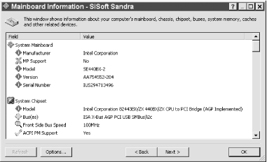 | Windows-based diagnostics programs either do not run or provide very limited functionality under Windows NT/2000, both of which limit access of applications to underlying hardware. If your system runs NT/2000, the best alternative is to boot DOS on it and run a DOS-based diagnostic utility. |
|
Identify the chipset visually by examining the motherboard. Most chipsets have two chips, although some have only one and a few have three or more. Look for relatively large, usually square chips that are labeled with the name of a chipset manufacturer Intel, VIA, SiS, ALi, Opti, etc. Record the string of numbers and letters that identifies each such chip. Then visit that manufacturer's web site and search for those strings to determine which chipset, if any, those chips belong to. For example, if you locate an Intel chip labeled 82438VX, a quick check of the Intel web site tells you that that chip is part of an Intel 430VX chipset (Intel calls most of its recent chipset models a PCIset or an AGPset). Note, however, that particularly on recent systems whose chipsets run at very high speeds, the chips that make up the chipset may have permanently installed heatsinks, which make it impossible to read the labels. 3.1.2.10 Fifth-Generation Chipsets Systems that use Intel fifth-generation chipsets are now too old to be upgraded effectively at the CPU/motherboard level, although such systems can sometimes usefully be upgraded by adding memory, a faster hard disk, and so on. Systems based on late-model third-party fifth-generation Super Socket 7 chipsets, such as the VIA MVP3, are still marginally upgradable by replacing the existing processor with a faster model, although Socket 7 processors are becoming rare and will likely disappear entirely by the end of 2002. Even if you have such a system that is technically upgradable, it is usually not cost-effective to do so. Instead, retire that system in situ to less demanding duties, and build a new system based on current technology. 3.1.2.11 Sixth-Generation Intel and Intel-Compatible Chipset Characteristics Intel has produced numerous sixth-generation chipsets in the 4-series and 8-series lines. Table 3-1 lists the characteristics of Intel 4-series desktop chipsets. These chipsets are obsolescent, although systems built on them may still be used productively and may even be reasonable upgrade candidates. In fact, motherboards based on the 440BX chipset were still being sold new as of June 2002. These chipsets do not support the most recent sixth-generation processors and lack modern features support for PC133 SDRAM and the 133 MHz FSB, PCI 2.2, fast ATA modes, 256 megabit memory chips, and so on but remain useful nonetheless.  | Processor support varies between steppings of chipsets, CPUs, and motherboards. For example, early steppings of the 815E chipset do not support Tualatin-core Pentium III and Celeron CPUs, while later steppings do. Similarly, some sixth-generation Intel chipsets support Covington-core and Mendocino-core Celerons, but not CoppermineT-core Celerons. Even if the chipset supports a particular CPU stepping, a motherboard that uses that chipset may not support that CPU. For detailed information about CPU support, see the Intel Specification Update for the chipset (http://developer.intel.com/design/chipsets/) and CPU (http://developer.intel.com/design/processor/) in question. |
|
Table 3-1. Intel 4-series sixth-generation chipset characteristics | | 440EX | 440LX | 440BX | 440ZX | 440ZX66 | | CPU support | | | | | | | Pentium II (66 FSB) | 
| | | | | | Pentium II (100 FSB) | 
| | | | | | Pentium III (100 FSB) | | | | | | | Pentium III (133 FSB) | | | | | | | Celeron (66 FSB) | | | | | | | Celeron (100 FSB) | | | | | | | Number of CPUs | 1 | 2 | 2 | 1 | 1 | | Host bus | | | | | | | 66 MHz | | | | | | | 100 MHz | | | | | | | 133 MHz | | | | | | | Memory support | | | | | | | EDO | 256 MB | 1 GB | | | | | PC66 SDRAM | 256 MB | 512 MB | 1 GB | 256 MB | 256 MB | | PC100 SDRAM | | | 1 GB | 256 MB | | | PC133 SDRAM | | | | | | | RDRAM | | | | | | | ECC support | | | | | | | 64/128/256 Mbit | / / | / / | / / | / / | / / | | EDO/SDRAM rows | 4 | 6 | 8 | 4 | 4 | | RDRAM devices | | | | | | | Asynchronous setting | | | | | | | PCI | | | | | | | PCI bus version | 2.1 | 2.1 | 2.1 | 2.1 | 2.1 | | Concurrent PCI | | | | | | | Southbridge | PIIX4E | PIIX4 | PIIX4E | PIIX4E | PIIX4E | | ATA support | 33 | 33 | 33 | 33 | 33 | | AGP support | | | | | | | Integrated graphics | | | | | | | 1X/2X/4X AGP | / / | / / | / / | / / | / / | Table 3-2 lists the characteristics of obsolescent and current Intel 8-series sixth-generation desktop chipsets. Intel has produced some chipsets in two versions, one using the Integrated Controller Hub (ICH) and the other using ICH2. The major differences between these versions are that ICH2 supports ATA100 (versus ATA66 for ICH) and provides two USB controllers with four USB ports (versus one controller/two ports for ICH). The ICH2 models did not replace the ICH models immediately. ICH models continued in production because Intel sold them for a few dollars less than ICH2 models. Every penny counts (literally) to mass-market vendors, who build PCs for the lowest possible cost and sell on very slim margins. Table 3-2. Intel 8-series sixth-generation chipset characteristics | | 810 | 810E/ 810E2 | 820/820E | 840 | 815/815E | | CPU support | | | | | | | Pentium II (100 FSB) | | | | | | | Pentium III (100 FSB) | | | | | | | Pentium III (133 FSB) | | | | | | | Celeron (66 FSB) | | | | | | | Celeron (100 FSB) | | | | | | | Number of CPUs | 1 | 1 | 1-2 | 1-2 | 1 | | Host bus | | | | | | | 66 MHz | | | | | | | 100 MHz | | | | | | | 133 MHz | | | | | | | Memory support | | | | | | | PC100 SDRAM | 512 MB | 512 MB | | | 512 MB | | PC133 SDRAM | | | | | 512 MB | | PC600 RDRAM | | | 1 GB | 8 GB | | | PC700 RDRAM | | | 1 GB | | | | PC800 RDRAM | | | 1 GB | 8 GB | | | Dual memory channel | | | | | | | ECC support | | | | | | | 64/128/256 Mbit | / / | / / | / / | / / | / / | | SDRAM rows | 4 | 4 | | | 6 | | RDRAM devices | | | 32 | 32 X 2 | | | Asynchronous setting | | | | | | | PCI | | | | | | | PCI bus version | 2.2 | 2.2 | 2.2 | 2.2 | 2.2 | | Concurrent PCI | | | | | | | Multiple PCI segments | | | | | | | Northbridge | 82810 | 82810E | 82820 (820) 82820E (820E) | 82840 | 82815 | | Southbridge | ICH | ICH (810E) ICH2 (810E2) | ICH (820) ICH2 (820E) | ICH | ICH (815) ICH2 (815E) | | ATA support | 66 | 66 (810E) 100 (810E2) | 66 (820) 100 (820E) | 66 | 66 (815) 100 (815E) | | AGP support | | | | | | | Integrated graphics | 82810 | 82810E | | | 82815 | | 1X/2X/4X AGP | / / | / / | / / | / / | / / | Intel intended the ill-starred 820 chipset to be the direct replacement for the venerable (and still respected) 440BX chipset. The 820 was a miserable failure, primarily because it was designed to use expensive Rambus RDRAM memory. With the 815 and the follow-on 815E, Intel finally got it right. The 815E is a superb chipset, fully worthy of inheriting the 440BX's crown as the best sixth-generation chipset available. The 815 and 815E chipsets are available in two variants. The 815 and 815E include an embedded graphics adapter. The 815P and 815EP do not. Figure 3-3 shows the Intel 815E, which is a representative Intel 8-series chipset. Intel calls the 82815 Northbridge the Graphics and AGP Memory Controller Hub (GMCH) and the 82801BA Southbridge the I/O Controller Hub (ICH2). Figure 3-1 early in this chapter showed the block diagram for the Intel 815E chipset. Figure 3-3. The Intel 815E chipset (image courtesy of Intel Corporation) 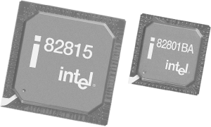 Intel makes the different 815 variants by mixing and matching the 82815 GMCH (Graphics and Memory Controller Hub) or the 82815EP MCH (Memory Controller Hub) with the 82801AA ICH (I/O Controller Hub) or the 82801BA ICH2 (I/O Controller Hub 2). Those variants with the MCH are designated "P" to indicate the absence of embedded graphics. Those that use the 82801BA are designated "E" to indicate the presence of the enhanced ICH2 Southbridge. The 815E has only two real limitations. First, it supports a maximum of 512 MB memory. At the time the 815E was designed, 512 MB was a reasonable limit. Few people could afford more. But with the plummeting price of RAM, 512 MB began to look like a real limitation. Second, the 815E officially supports only one CPU (although at least one motherboard maker, Acorp, has produced a dual-CPU 815E motherboard). If the 815E supported 1 GB or more of memory and dual processors, it would be the perfect sixth-generation chipset for Intel processors. As it is, the 815E is merely the best available. | Although Intel originally claimed SDRAM support for the 820 chipset, they implemented that support via the Memory Translator Hub (MTH). After many motherboards had been shipped, Intel found that the MTH corrupted data. Intel recalled the CC820 motherboard, which was the only SDRAM 820-based motherboard they produced. Third-party motherboard makers also recalled their 820-based SDRAM motherboards. However, as with any recall, not everyone returned the boards, so you may still encounter 820-based motherboards that use SDRAM. If you discover such a board, stop using it immediately. Using it risks your data. |
|
Other companies, including VIA Technologies, Inc., Acer Laboratories, Inc. (ALi), and Silicon Integrated Systems (SiS), make chipsets for Intel sixth-generation CPUs. In our experience, these third-party chipsets are slower, buggier, less compatible, and less stable than Intel chipsets. So why would any motherboard maker use them? Three reasons: - Price
-
Third-party chipsets generally sell for $5 or $10 less than Intel chipsets. If you are building a motherboard to a price-point, the difference between a $40 Intel chipset and a $30 third-party chipset is huge. Although we won't say that all motherboards with non-Intel chipsets are built with cost as the only priority, it is certainly a significant issue. - Feature sets
-
Intel is conservative about adding support for new technologies to their chipsets. So, for example, when DDR-SDRAM became all the rage, Intel did not produce a chipset that supported it, so motherboard makers who wanted to produce DDR-SDRAM motherboards had no choice but to use a third-party chipset. Similarly, the last mainstream SMP-capable chipset Intel produced was the 440BX, which lacks support for such essentials as the 133 MHz FSB. Motherboard makers who want to produce a modern dual Pentium III board have little choice but to use a third-party chipset like the VIA Apollo Pro133A or Apollo Pro266. - Availability
-
Despite their higher costs and more limited feature sets, most motherboard makers want Intel chipsets because they perceive (rightly) that Intel chipsets are superior to those produced by other manufacturers. Intel's production capacity, while large, is not unlimited. When Intel ships a new chipset, they are often unable to meet demand. Third-party manufacturers step in with chipsets that have comparable features and are available immediately in volume. Figure 3-4 shows the block diagram for a typical third-party chipset, in this case the VIA Apollo Pro266T, which supports Intel sixth-generation processors. Figure 3-4. Block diagram of the VIA Apollo Pro266T chipset (graphic courtesy of VIA Technologies, Inc.) 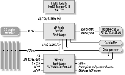 Of the third-party chipset makers, VIA Technologies is the largest and most prolific. VIA chipsets are found in motherboards made by nearly every major motherboard maker other than Intel, including such premier Taiwanese makers as ASUS, EPoX, and Gigabyte. Figure 3-5 shows the two chips that make up the VIA Apollo Pro266, a representative VIA chipset. The VT8633 chip is the Northbridge and the VT8233 is the Southbridge. As does Intel, VIA mixes and matches various Northbridges and Southbridges from within a given family to produce related chipsets with different features. Figure 3-5. The VIA Apollo Pro266 chipset (image courtesy of VIA Technologies, Inc.) 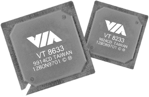 Table 3-3 lists the characteristics of several VIA chipsets for Intel sixth-generation processors. The PM601 and Pro133 chipsets are obsolescent. The Pro133A and Pro266 are used in current motherboards. VIA produces variants of these chipsets, which differ chiefly in terms of processor support and whether or not embedded graphics are included. For example, the Apollo Pro133A chipset is also available as the Pro133T, which adds support for Tualatin-core Pentium III processors, and as the PM133, which adds embedded Savage video to the Pro133A chipset. Similarly, the PL133T is based on the Pro133A chipset, but includes Tualatin support and embedded Savage video. As always, the Northbridge determines which processors and memory types are supported, and the Southbridge determines which peripherals are supported. Table 3-3. Characteristics of VIA chipsets for sixth-generation Intel processors | | PM601 | Pro133 | Pro133A | Pro266 | | CPU support | | | | | | Pentium II (66 FSB) | | | | | | Pentium II (100 FSB) | | | | | | Pentium III (100 FSB) | | | | | | Pentium III (133 FSB) | | | | | | Celeron (66 FSB) | | | | | | Celeron (100 FSB) | | | | | | Number of CPUs | 1 | 1 | 1-2 | 1-2 | | Host bus | | | | | | 66 MHz | | | | | | 100 MHz | | | | | | 133 MHz | | | | | | Memory support | | | | | | EDO | | 1.5 GB | 1.5 GB | | | PC66 SDRAM | 1 GB | 1.5 GB | 1.5 GB | 4 GB | | PC100 SDRAM | 1 GB | 1.5 GB | 1.5 GB | 4 GB | | PC133 SDRAM | 1 GB | 1.5 GB | 1.5 GB | 4 GB | | VC133 SDRAM | 1 GB | 1.5 GB | 1.5 GB | 4 GB | | PC1600 DDR-SDRAM | | | | 4 GB | | PC2100 DDR-SDRAM | | | | 4 GB | | RDRAM | | | | | | Dual memory channel | | | | | | ECC support | | | | | | 64/128/256 Mbit | / / | / / | / / | / / | | EDO/SDRAM rows | 4 | 4 | 4 | 4 | | RDRAM devices | | | | | | Asynchronous setting | | | | | | PCI | | | | | | PCI bus version | 2.2 | 2.2 | 2.2 | 2.2 | | Concurrent PCI | | | | | | Multiple PCI segments | | | | | | Northbridge | VT82C601 | VT82C693A | VT82C694X | VT8633 | | Southbridge | VT82C686A | VT82C596B VT82C686A | VT82C596B VT82C686A | VT8233 | | ATA support | 100 | 66 | 66 | 100 | | AGP support | | | | | | Integrated graphics | Blade3D | | | | | 1X/2X/4X AGP | / / | / / | / / | / / | ALi and SiS chipsets for Intel sixth-generation processors sell in smaller numbers and are less widely used. Against Intel and VIA, which between them overwhelmingly dominate the chipset market, ALi and SiS must compete largely on price, so their chipsets are usually found in inexpensive motherboards intended for mass-market systems. For Intel processors, we recommend using motherboards based on Intel chipsets whenever possible. If you need a feature that is unavailable with an Intel chipset, choose a VIA-based motherboard. If you encounter an ALi- or SiS-based motherboard, visit http://www.acerlabs.com/ or http://www.sis.com/ for detailed information about their chipsets. 3.1.2.12 AMD Athlon Chipset Characteristics The AMD Athlon and Duron are good sixth-generation processors that have been hampered by mediocre chipsets. Considered in isolation, the Athlon is at least as good as the Pentium III, and the Duron is in most respects better than the Celeron. But you can't use a processor without a chipset, and inferior chipsets have plagued AMD processors since their introduction. The first Athlon chipset, the AMD-750 "Irongate," was intended by AMD as a technology demonstrator rather than as a production chipset. AMD didn't want to be in the chipset or motherboard business, although we don't understand that decision. They'd always intended that production chipsets for their processors would be manufactured by VIA, ALi, and SiS. But VIA was very late to market with their first Athlon chipset, the KX133, so AMD was forced to produce the Irongate in volume for early Athlon motherboards. The situation has improved since those early days. The majority of Athlon/Duron motherboards now use one or another VIA chipset, and the quality of subsequent VIA chipsets has improved. Current VIA chipsets are usable, if not quite up to Intel chipsets in terms of performance, compatibility, and stability. AMD produces the excellent AMD-760 series of chipsets, which we regard as equivalent in quality to Intel chipsets. Table 3-4 lists the characteristics of three first- and second-generation VIA chipsets for the Athlon/Duron, with the AMD-750 shown for comparison. The AMD-750 and VIA KX133 are obsolete first-generation chipsets. The VIA KT133 is an obsolescent early second-generation chipset. The KT133A and its derivatives like the KM133 remain in production as VIA's primary Athlon/Duron SDR-SDRAM chipsets. The KT133A is as fast or faster with SDR-SDRAM than the third-generation KT266 with SDR-SDRAM, and nearly as fast as the KT266A with DDR-SDRAM. ALi and SiS have also produced second-generation Athlon chipsets, but we recommend avoiding any motherboard that uses them. Note that a nominal 200 MHz FSB speed is actually a double-pumped bus running at 100 MHz, and a nominal 266 MHz FSB speed is actually 133 MHz double-pumped. Table 3-4. Athlon/Duron SDR-SDRAM chipset characteristics | | AMD 750 | VIA KX133 | VIA KT133 | VIA KT133A | | CPU support | | | | | | Slot A / Socket A | / | / | / | / | | Athlon / Duron | / | / | / | / | | 66/100/133 MHz FSB | / / | / / | / / | / / | | Number of CPUs | 1 | 1 | 1 | 1 | | Memory bus | | | | | | 66 MHz | | | | | | 100 MHz | | | | | | 133 MHz | | | | | | Memory support | | | | | | PC100 SDRAM | 768 MB | 2 GB | 1.5 GB | 1.5 GB | | PC133 SDRAM | | 2 GB | 1.5 GB | 1.5 GB | | VC133 SDRAM | | 2 GB | 1.5 GB | 1.5 GB | | PC1600 SDRAM | | | | | | PC2100 SDRAM | | | | | | ECC | | | | | | 64/128/256 Mbit | / / | / / | / / | / / | | SDRAM rows | 3 | 4 | 4 | 4 | | Asynchronous setting | | | | | | PCI | | | | | | PCI bus version | 2.2 | 2.2 | 2.2 | 2.2 | | Concurrent PCI | | | | | | Northbridge | | 8371 | 8363 | 8363A | | Southbridge | AMD-756 | 82C686A | 82C686A | 82C686B | | ATA support | 66 | 66 | 100 | 100 | | AGP support | | | | | | Integrated graphics | | | | | | 1X/2X/4X AGP | / / | / / | / / | / / | | VIA originally named the KT133 the KZ133, but later changed the name because KZ was the abbreviation used by the Nazis for concentration camps. This change occurred just before the chipset shipped in volume, and some motherboards were produced with chipsets labeled KZ133. If you encounter such a motherboard, treat it as a KT133 model. |
|
The availability of Double Data Rate SDRAM (DDR-SDRAM) resulted in a flurry of new Athlon/Duron chipset designs from AMD, VIA, and other makers. In fact, for sixth-generation processors like the Athlon and Duron (as well as the Pentium III and Celeron) DDR-SDRAM is more marketing hype than substance. Sixth-generation processors are seldom bound by memory bandwidth, so doubling bandwidth results in relatively minor overall performance benefits. Still, DDR-SDRAM is the wave of the future, so all of the chipset makers jumped on board. Figure 3-6 shows a block diagram of the VIA KT266 chipset, their first chipset for AMD processors that supports DDR-SDRAM. Figure 3-6. Block diagram of the VIA Apollo KT266 chipset (graphic courtesy of VIA Technologies, Inc.) 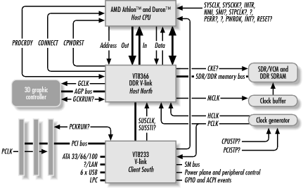 Table 3-5 lists the characteristics of DDR-SDRAM capable chipsets, which we define as third-generation Athlon chipsets. The AMD-760 and ALi Magik1 shipped in production quantities in February 2001 (although the AMD-760 had shipped in low volumes the previous fall), and the VIA KT266, SiS 735, AMD-760MP, and AMD-760MPX in April, May, June, and December 2001, respectively. Motherboards based on all of these chipsets except the AMD-760MPX began shipping in volume in summer and fall 2001. Motherboards based on the AMD-760MPX began shipping in volume in early 2002. These chipsets differ architecturally but are similar in most functional respects. All, for example, support all current Socket 462 AMD processors, six PCI slots, and at least a subset of the full ACPI specification. All support six USB 1.1 ports except the AMD chipsets, which support four. None supports ATA133, Serial ATA, USB 2.0, or other recent standards promoted by Intel. Table 3-5. Athlon/Duron DDR-SDRAM chipset characteristics | | AMD 760 | AMD 760MP | AMD 760MPX | VIA KT266 | VIA KT266A | ALi Magik1 | SiS 735 | SiS 745 | | CPU support | | | | | | | | | | Slot A / Socket A | / | / | / | / | / | / | / | / | | Athlon / Duron | / | / | / | / | / | / | / | / | | 66/100/133/166 MHz FSB | / / / | / / / | / / / | / / / | / / / | / / / | / / / | / / / | | Number of CPUs | 1 | 2 | 2 | 1 | 1 | 1 | 1 | 1 | | Memory bus | | | | | | | | | | 100 MHz | | | | | | | | | | 133 MHz | | | | | | | | | | Memory support | | | | | | | | | | PC133 SDRAM | | | | 2 GB | 2 GB | 1 GB | 1.5 GB | | | VC133 SDRAM | | | | | | | | | | PC1600 SDRAM | 2 GB | 3 GB | 4 GB | 2 GB | 2 GB | 1 GB | 1.5 GB | 3 GB | | PC2100 SDRAM | 2 GB | 3 GB | 4 GB | 2 GB | 2 GB | 1 GB | 1.5 GB | 3 GB | | PC2700 SDRAM | | | | | | | | 3 GB | | ECC | | | | | | | | | | 64/128/256 Mbit | / / | / / | / / | / / | / / | / / | / / | / / | | SDRAM rows | 4 | 4 | 4 | 4 | 4 | 4 | 3 | 3 | | Asynchronous setting | | | | | | | | | | PCI | | | | | | | | | | PCI bus version | 2.2 | 2.2 | 2.2 | 2.2 | 2.2 | 2.2 | 2.2 | 2.2 | | Concurrent PCI | | | | | | | | | | Northbridge | AMD-761 | AMD-762 | AMD-762 | VT8366 | VT8366A | M1647 | SiS735 | SiS745 | | Southbridge | AMD-766 | AMD-766 | AMD-768 | VT8233 | VT8233 | M1535D+ | (none) | (none) | | ATA support | 100 | 100 | 100 | 100 | 100 | 100 | 100 | 100 | | AGP support | | | | | | | | | | Integrated graphics | | | | | | | | | | 1X/2X/4X AGP | / / | / / | / / | / / | / / | / / | / / | / / | The AMD-760, AMD-760MP, and AMD-760MPX are the premium chipsets in this group, and they are priced accordingly. All offer high performance and stability, and the MP and MPX versions are of course the only chipsets available that support dual AMD processors. The MP and MPX chipsets differ only in the Southbridge they use. The MPX differs in two respects from the MP, one minor and one major. The minor difference is that the MPX includes embedded AC97 audio. The major difference is in their PC buses. The MP provides one 32/64-bit 33 MHz PCI bus. The MPX supports two PCI buses. The primary PCI bus is a 33/66 MHz, 32/64-bit bus, which is used for communications between the AMD-762 Northbridge and the AMD-768 Southbridge, and is also extended to provide one or two high-performance 64-bit PCI expansion slots. The secondary PCI bus is a 33 MHz 32-bit bus, which is used for standard 32-bit PCI peripheral cards. The primary PCI bus doubles throughput between the Northbridge and Southbridge relative to the single 33 MHz 32/64-bit PCI bus used in the AMD-760. | Be careful when configuring a system based on a motherboard with an AMD-760MPX chipset. It's possible to cripple system performance without even realizing you've done so. The primary PCI bus is a dual-speed, dual-width bus, which is really intended to operate at 66 MHz with a 64-bit bandwidth. Installing a 32-bit PCI card in one or both of the high-performance PCI slots forces the primary bus to operate in 32-bit mode rather than 64-bit mode. Similarly, installing a 33 MHz PCI card in either or both of the two high-performance slots forces the primary PCI bus to operate in 33 MHz mode rather than 66 MHz mode. Even if you never plan to install a 66 MHz 64-bit PCI card, forcing the primary PCI bus to operate more slowly halves the throughput between the Northbridge and Southbridge. Keep those 66 MHz 64-bit slots open unless you are installing a 66 MHz 64-bit expansion card in them. |
|
Unfortunately, supplies of AMD chipsets are likely to be limited. For some reason, AMD prefers to leave chipset manufacturing to third parties, and produces their own chipsets only to "seed" the market. Also, although dual-CPU motherboards based on the AMD-760MP are readily available, and AMD-760MPX motherboards will ship in volume during 2002, no motherboard maker currently produces a true AMD-760 uniprocessor motherboard. Some are advertised as such, but all of those in fact use only the AMD-761 Northbridge, substituting a VIA Southbridge for the AMD-766. Manufacturers do this to save a few bucks, but the resulting motherboards are not stable enough for us to recommend. The VIA KT266 and ALi Magik1 are run-of-the-mill chipsets. There's nothing special about either of them. Both provide a standard set of features, acceptable though not outstanding performance, and reasonable stability (although early versions of the Magik1 had numerous performance and stability problems). Both are targeted squarely at the mass market, and both compete largely on price with the superior chipsets from AMD. We don't consider either of them a particularly good choice. The VIA KT266A is an enhanced version of the KT266, which provides deeper internal buffers and a much-improved memory controller. Taken together, these improvements allow the KT266A to match or exceed the performance of the AMD 760 and SiS 735 chipsets, but our concerns about the stability and compatibility of VIA chipsets remain. The real surprise is the SiS 735. SiS chipsets do not have a reputation for high performance or stability. They're typically found in bargain-basement systems, where their low price is a fair trade-off for lower performance. With the 735, however, SiS got it right. The 735 is actually faster than the AMD-760, and seems to be just as stable, which we frankly find astonishing. The only problem with the SiS 735 is finding one. Just as Intel has used its clout to discourage motherboard makers from using VIA chipsets, VIA has discouraged Athlon/Duron motherboard manufacturers from using SiS chipsets. As a result, few first- or second-tier Taiwanese makers offer SiS 735-based motherboards. Some SiS 735 boards are made by manufacturers whose products we wouldn't touch with a barge pole, so our favorable opinion of the SiS 735 doesn't extend to all motherboards that use it. Fortunately, though, there is at least one good choice, which we describe on our web site. SiS also produces the follow-on SiS 745, which we have not yet had the opportunity to test. | The much-hyped nVIDIA nForce chipsets turned out to be a disappointment. For example, the respected Tom's Hardware Guide concluded, "KT266A Trounces nForce 420D." As of early 2002, very few motherboards based on the nVIDIA chipsets were shipping, and we had not yet been able to obtain any for testing. We think the high cost and mediocre performance of the nForce combined with the inexperience of nVIDIA in the chipset market dooms this chipset to failure. But we've been wrong before. |
|
3.1.2.13 Seventh-Generation Intel and Intel-Compatible Chipset Characteristics Although AMD tried to represent the Athlon as a seventh-generation processor, (hence the initial designation of the Athlon as the K7), the first true seventh-generation processor is the Intel Pentium 4. The Pentium 4 differs architecturally from sixth-generation processors dramatically, so chipsets designed for the Pentium 4 are not merely minor upgrades of sixth-generation chipsets. The first Pentium 4 chipset, the Intel 850, is shown in Figure 3-7. Figure 3-7. Block diagram of the Intel 850 chipset (graphic courtesy of Intel Corporation) 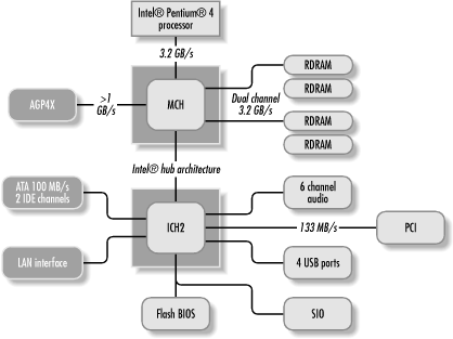 Current Pentium 4 chipsets are differentiated chiefly by the type of memory they support. Sixth-generation processors like the Intel Pentium III and AMD Athlon do not benefit greatly from the higher bandwidth of Rambus RDRAM and Double Data Rate SDRAM (DDR-SDRAM). Under most circumstances, the 1,067 MB/s bandwidth of PC133 SDRAM can more or less keep up with the memory bandwidth requirements of these processors. (See the upcoming Table 3-6.) The Pentium 4, on the other hand, can productively use more memory bandwidth than PC133 can provide. Using PC133 with a Pentium 4 cripples it by forcing it to spend a large percentage of its time waiting for slow memory to supply data. For that reason, the Pentium 4 is better matched with a faster memory technology like Rambus RDRAM or DDR-SDRAM. Rambus RDRAM is available in three speeds, called PC600, PC700, and PC800, which provide 1,200 MB/s, 1,400 MB/s, and 1,600 MB/s memory bandwidth respectively. The Intel 850 chipset supports two channels of RDRAM, for maximum throughput of 3.2 GB/s. That data rate is also the design bandwidth of the Pentium 4, which runs a quad-pumped 100 MHz FSB (for an effective 400 MHz FSB) with 64-bit (8-byte) memory transfers. Transferring eight bytes 400 million times per second translates to 3.2 GB/s. DDR-SDRAM is available in three speeds, called PC1600 (or DDR200), PC2100 (DDR266), and PC2700 (DDR333), which provide 1,600 MB/s, 2,100 MB/s, and 2,700 MB/s memory bandwidth respectively. Even 2,700 MB/s falls short of the 3.2 GB/s bandwidth of the Pentium 4, but that's less an issue than it might seem. Very few applications require the full memory bandwidth of the Pentium 4, so although PC133 bandwidth may hamper the Pentium 4 in normal operations, few applications require more bandwidth than PC1600 or PC2100 DDR-SDRAM provides. Although nothing prevents designing a dual-channel DDR-SDRAM chipset to provide 3.2 GB/s, 4.2 GB/s, or 5.2 GB/s bandwidth using current DDR-SDRAM modules, such a chipset does not (yet) exist. As later generations of the Pentium 4 will use a quad-pumped 133 MHz FSB for throughput of 4.2 GB/s or a quad-pumped 166 MHz FSB for 5.2 GB/s, it's possible that later generations of Pentium 4 chipsets will in fact adopt a dual-channel memory structure. For now, though, standard DDR-SDRAM is sufficient for nearly any Pentium 4 application. Table 3-6. Characteristics of first-generation chipsets for the Intel Pentium 4 | | Intel 850 | Intel 845 | VIA P4X266 | SiS 645 | ALi ALADDiN-P4 | | CPU support | | | | | | | PGA 423 (Willamette) | | | | | | | mPGA 478 (Willamette) | | | | | | | mPGA 478 (Northwood) | | | | | | | Number of CPUs | 1-2 | 1 | 1 | 1 | 1 | | Host bus | | | | | | | 100 MHz (quad pumped) | | | | | | | Memory support | | | | | | PC133 SDR-SDRAM | | 3 GB | 4 GB | 3 GB | 3 GB | | VC133 SDRAM | | | 4 GB | | | | PC1600 DDR-SDRAM | | 2 GB | 4 GB | | 3 GB | | PC2100 DDR-SDRAM | | 2 GB | 4 GB | 3 GB | 3 GB | | PC2700 DDR-SDRAM | | | | 3 GB | 3 GB | | PC600 RDRAM | 2 GB | | | | | | PC700 RDRAM | | | | | | | PC800 RDRAM | 2 GB | | | | | | Dual memory channel | | | | | | | ECC support | | | | | | | 64/128/256/512 Mbit | / / / | / / / | / / / | / / / | / / / | | SDR/DDR SDRAM rows | | 6 / 4 | 4 / 4 | 3 / 3 | 6 / 4 | | RDRAM devices | 32 X 2 | | | | | | Asynchronous setting | | | | | | | PCI | | | | | | | PCI bus version | 2.2 | 2.2 | 2.2 | 2.2 | 2.2 | | Concurrent PCI | | | | | | | Multiple PCI segments | | | | | | | Northbridge | 82850 | 82845 | VT8753 | SiS645 | M1671 | | Southbridge | 82801BA | 82801BA | VT8233 | SiS961 | M1535D+ | | ATA support | 100 | 100 | 100 | 100 | 100+ | | AGP support | | | | | | | Integrated graphics | | | | | | | 1X/2X/4X AGP | / / | / / | / / | / / | / / | | There's an odd situation that we call "the chipset that never was." Reviews and online PC enthusiast sites discuss the Intel 845 and "845D" chipsets as though they were two distinct products. In fact, there has been only one Intel 845 chipset, and Intel has never produced an 845D. Early steppings of the 845 were not certified for use with DDR-SDRAM, but later steppings can support either SDR or DDR-SDRAM interchangeably. Intel released several new variants of the 845, called the 845E, 845G, and 845GL, in May 2002. These second-generation 845-series chipsets are detailed in Table 3-7 . |
|
Table 3-7. Characteristics of second-generation chipsets for the Intel Pentium 4 | | Intel 850E | Intel 845E | Intel 845G | Intel 845GL | | CPU support | | | | | | PGA 423 (Willamette) | | | | | | mPGA 478 (Willamette) | | | | | | mPGA 478 (Northwood) | | | | | | mPGA 478 (Willamette128) | | | | | | Number of CPUs | 1-2 | 1 | 1 | 1 | | Host bus | | | | | | 100 MHz (quad pumped) | | | | | | 133 MHz (quad pumped) | | | | | | Memory support | | | | | | PC133 SDR-SDRAM | | | 2 GB | 2 GB | | VC133 SDRAM | | | | | | PC1600 DDR-SDRAM | | 2 GB | 2 GB | 2 GB | | PC2100 DDR-SDRAM | | 2 GB | 2 GB | 2 GB | | PC2700 DDR-SDRAM | | | 2 GB | | | PC600 RDRAM | | | | | | PC700 RDRAM | | | | | | PC800 RDRAM (45 ns) | 2 GB | | | | | PC800 RDRAM (40 ns) | 2 GB | | | | | PC1066 RDRAM | | | | | | Dual memory channel | | | | | | ECC support | | | | | | 64/128/256/512 Mbit | / / / | / / / | / / / | / / / | | SDR/DDR SDRAM rows | | 0 / 4 | 4 / 4 | 4 / 4 | | RDRAM devices | 32 X 2 | | | | | Asynchronous setting | | | | | | PCI | | | | | | PCI bus version | 2.2 | 2.2 | 2.2 | 2.2 | | Concurrent PCI | | | | | | Multiple PCI segments | | | | | | Northbridge | 82850E | 82845E | 82745G | 82845GL | | Southbridge | 82801BA | 82801DB | 82801DB | 82801DB | | ATA support | 100 | 100 | 100 | 100 | | USB 1.1 / 2.0 support | / | / | / | / | | AGP support | | | | | | Integrated graphics | | | | | | 1X/2X/4X AGP | / / | / / | / / | / / | Table 3-7 lists second-generation Intel P4 chipsets. Although Intel was not expected to ship the 850E chipset, codenamed Tehama-E, until fall 2002, they released that chipset in May 2002. Originally, the 850E was supposed to use the 82801DB/82801CA Southbridge (ICH4), which adds USB 2.0 support, but the 850E instead uses the same 82801BA (ICH2) Southbridge used in the original 850 chipset. The 850E is thus really not a new chipset at all, but merely a revision of the 850 chipset that Intel certifies for operation with the 533 MHz FSB. In fact, late steppings of the 850 chipset may support 533 MHz operation, although Intel does not sanction using the 850 at 533 MHz. Intel did not initially qualify the 850E for use with PC1066 RDRAM because PC1066 RDRAM was not yet shipping when the 850E was introduced. However, we have been told unofficially that the 850E does support PC1066 RDRAM, and expect later steppings of the 850E to add official support for PC1066 RDRAM. Intel had also originally scheduled a fall 2002 release for several new variants of the 845 chipset, but again moved that release forward to May 2002, when they introduced the following chipsets: - 845E (Brookdale-E)
-
The 845E chipset differs in two major respects from the original 845 chipset. The 845E adds support for the 533 MHz FSB, and replaces the 82801BA (ICH2) Southbridge of the 845 with ICH4, which adds support for USB 2.0. Like the 845 chipset, the 845E supports PC133 SDR-SDRAM and PC1600/PC2100 DDR-SDRAM, but not PC2700 DDR-SDRAM. - 845G (Brookdale-G)
-
The 845G chipset supports the 533 MHz FSB and USB 2.0, and adds embedded graphics with 3D performance comparable to the nVIDIA GeForce2/MX400. In effect, the 845G is the Pentium 4 version of the popular Pentium III 815E chipset. Like the 815E, the 845E supports an AGP 4X slot, which allows the video to be upgraded by adding a standard AGP card. The 845G is the first Intel chipset that supports PC2700 DDR-SDRAM. - 845GL (Brookdale-GL)
-
The 845GL chipset is the "lite" version of the 845G, and is intended for budget systems that use P4-based Celeron processors. Intel introduced the 845GL chipset at $30, a very low price for an Intel chipset, and one targeted at taking away "value segment" market share from Taiwanese chipset makers. The 845GL has the same embedded graphics as the 845G, but unlike the 845G, the 845GL does not support an external AGP connector. Nor does the 845GL support the 533 MHz FSB or PC2700 DDR-SDRAM, although it does use ICH4 and therefore supports USB 2.0. The Intel 850E and 845E/G/GL chipsets are the best chipsets available for the Pentium 4 and P4-based Celeron. These chipsets are fast and immensely stable, and, like most Intel chipsets, have few compatibility problems compared to competing chipsets. If your application demands the highest possible memory performance which few applications really do require choose a board based on the 850E and Rambus RDRAM, but realize that doing so gives up the advantages of ICH4 and USB 2.0. We see no reason to choose the 845E chipset. Although it does support the 533 MHz FSB and USB 2.0, the 845E lacks the embedded graphics and PC2700 support of the 845G chipset, and sells for only a few dollars less. For mainstream systems, choose an 845GL motherboard with PC2100 or (better) PC2700 DDR-SDRAM. Although, like all Intel chipsets, the 845GL has excellent performance and stability, we avoid it because of its functional limitations unless price is a very high priority. In that case, choose an 845GL-based motherboard with a Celeron and PC2100 DDR-SDRAM, but recognize that the absence of an AGP slot means you won't be able to upgrade the video later. 3.1.3 BIOS By themselves, the processor, memory, chipset, and other motherboard components are a useless collection of silicon, plastic, and metal. None of them individually can do much without help from other components, and none of them knows how to talk to other components. Turning this random collection of parts into a functioning computer requires a BIOS, or Basic Input/Output System. The BIOS is a real-mode program that is more or less permanently stored on a chip that resides on the motherboard. Originally, the BIOS was stored on a ROM (Read-Only Memory) chip, hence the term ROM BIOS. The only way to upgrade a ROM BIOS is to physically remove that chip and install a new one. Nowadays, the BIOS resides on a Programmable ROM (PROM), which allows the BIOS code to be updated without physically replacing the chip. When power is applied to the system board, the CPU initializes. The final step in its hardcoded initialization routine is to jump to a predefined memory address and execute the program that it finds there. That address is the entry point for the BIOS code, so as the CPU finishes initializing, the BIOS code begins executing the system boot sequence. To begin, the BIOS initializes installed hardware and performs the power-on self test (POST). At the conclusion of the system boot sequence, the BIOS loads the operating system and passes control to it. Once the operating system loads, the BIOS may also perform various low-level system services at the request of the operating system or applications. Operating systems like DOS and Windows 3.X depend relatively heavily on the BIOS to provide standardized basic services. But the BIOS is a slow real-mode program, so newer operating systems like Windows 95/98/NT/2000/XP and Linux depend less on BIOS services and more on drivers that access the hardware directly. | Most PCs contain several BIOSes. This discussion refers to the main system BIOS, but most network adapters, video adapters, and disk host adapters contain their own specialized BIOSes. When the system boots, the main BIOS detects the presence of these specialized BIOSes and loads them, allowing the PC to support that hardware by using the program routines contained on that BIOS. Using one of these BIOSes may be automatic or optional. For example, some SCSI host adapters contain a BIOS. If you load that BIOS at boot time, you can boot from a SCSI drive attached to that adapter. If you do not load that BIOS, you cannot boot from or access the SCSI device until the operating system loads the device drivers needed to recognize it. |
|
One major function of the BIOS is to intermediate between the chipset, the CPU, and other major system components. Full implementation of some system-level features things like USB, Plug-N-Play, Power Management, and AGP requires support from both the chipset and the BIOS. If either lacks support for a feature, that feature is either unavailable or has limited functionality. Most PCs and motherboards use BIOSes made by Phoenix, American Megatrends, Inc. (AMI), or Award (now a subsidiary of Phoenix). Some name-brand PCs like IBM and Compaq use a BIOS with that manufacturer's name on it, although that BIOS is usually a relabeled Phoenix, AMI, or Award BIOS, with or without minor modifications. When you buy a new PC or motherboard, the BIOS it uses is relatively unimportant, certainly much less so than the chipset it uses. You can safely assume that the BIOS on any new PC or motherboard will support all or most of the chipset capabilities. There may be minor exceptions for example, some early systems with USB ports came with BIOSes that did not support USB but such exceptions are usually unimportant to the overall functioning of the system. Also, unlike the chipset, the BIOS in a modern PC can be upgraded easily to fix bugs and to support new hardware and additional features. 3.1.4 Processor Support Motherboards are designed to accept a particular processor (CPU) or CPU family. Which CPUs a motherboard supports is determined by: - Chipset
-
Determines the CPU types the motherboard accepts. Non-Intel chipsets typically support a wide range of Intel and compatible CPUs. Officially, Intel chipsets support only Intel CPUs. In fact, compatible CPUs like the AMD K5/K6/K6-2, the Cyrix/IBM 6x86 (M1) and 6x86MX (M2), and the IDT WinChip run fine in motherboards with the appropriate Intel chipset. Also, although recent compatible CPUs can be installed in motherboards with older chipsets, those CPUs may not provide the highest performance of which they are capable, and some advanced features may not be supported by the chipset. The chipset also determines the fastest CPU that the motherboard can support. Intermediate speeds may or may not be supported, depending on the configuration options available for the motherboard. - CPU voltages supplied
-
Early Pentium-class CPUs use 5 volts. Later ones use 3.3 volts or 2.8 volts, and most later Pentium-class CPUs use dual voltage, running the internal core logic at a lower voltage than the CPU components that interface with cache, main memory, and other external components. Early fifth-generation motherboards supplied a fixed voltage to the CPU. Later ones included a voltage regulator module (VRM) that allowed the motherboard to be configured to supply different voltages, according to the requirements of the CPU installed. Some non-Intel Socket 7 motherboards allow specifying core voltage and I/O voltage separately, using very small increments. A motherboard like this can be tweaked to provide exactly the voltage required by a particular CPU. Sixth-generation CPUs may use 2.8 volts (e.g., Klamath-core Pentium II), 2.0 volts (e.g., Deschutes-core Pentium II), 1.6 volts (most current sixth-generation processors), or less, and seventh-generation processors are rapidly heading for the sub-1V level. As processor fabrication transitions from the 0.18 process to 0.13 and later 0.10, you can expect processor voltages to decline in lockstep. Sixth- and seventh-generation motherboards automatically detect and supply the voltage required by the processor, but you should verify that a particular motherboard can supply the voltages required by a particular processor before you install that processor. | Just because a motherboard supplies the nominal voltage used by a given processor does not mean that processor can be used with that motherboard. Available current is also an issue. For example, early versions of the Intel SE440BX Seattle motherboard provide the 2.0 volts used by Deschutes-core Pentium IIs and Katmai-core Pentium IIIs. But the VRM on early SE440BXs cannot supply the higher current required by the Pentium III. Attempting to run a Pentium III in the motherboard may damage both motherboard and processor. Before you install or upgrade a processor in any motherboard, always check the technical documents to verify that that processor is supported by that motherboard. Even if the processor appears to work initially, it may be drawing more current than the motherboard can supply, which may damage the motherboard and the processor. |
|
- Configuration options and memory bus speed
-
A motherboard may not support the necessary settings for bus speed and/or CPU multiplier for a particular CPU. For example, a motherboard that offers only 50, 60, and 66 MHz bus speeds will not properly support a CPU that uses a 75 MHz bus, although it may physically accept it, and a Pentium II motherboard that supports only 66 MHz FSB cannot use a Pentium II CPU that requires a 100 MHz FSB. In such cases, the processor will normally operate properly, but at some fraction of its rated speed. Similarly, a Pentium III/Celeron or Athlon/Duron motherboard that supports only the 100 MHz FSB may be able to use a 133 MHz FSB processor, but will run it at only 3/4 (100/133) of its rated speed. - Socket or Slot
-
Determines which CPU packaging styles fit the motherboard. Table 3-8 lists the socket and slot types you may encounter. New motherboards are available for Socket 7 and Socket 8 (both obsolete), Slot 1, Slot A, and Socket 423 (all obsolescent), Socket 370, Socket A, and Socket 478. Table 3-8. Desktop processor sockets and slots | | Pins | Voltage | Processors supported | | Socket 1 | 169 | 5 | 486 | | Socket 2 | 238 | 5 | 486-SX; SX/2; DX; DX/2; DX/4 | | Socket 3 | 237 | 5 / 3.3 | 486-SX; SX/2; DX; DX/2; DX/4; 486 Pentium Overdrive | | Socket 4 | 273 | 5 | Pentium 60/66; Pentium 60/66 Overdrive | | Socket 5 | 320 | 3.3 | Pentium 75-300; Pentium 75+ Overdrive | | Socket 6 | 235 | 3.3 | (Never used) | | Socket 7 | 321 | VRM | Pentium 75-300; Pentium 75+ Overdrive | | Socket 8 | 387 | VRM | Pentium Pro | | Socket 370 | 370 | VRM | PPGA Celeron, FC-PGA Pentium III | | Slot 1 | 242 | VRM | Pentium II, Celeron, Pentium III | | Slot A | 242 | VRM | AMD Athlon (slotted version) | | Socket A | 462 | VRM | AMD Thunderbird/Duron (socketed) | | Socket 423 | 423 | VRM | Intel Pentium 4 (early versions) | | Socket 478 | 478 | VRM | Intel Pentium 4 and Celeron (current versions) | Identifying the socket type on an existing motherboard may or may not be simple. Most sockets are labeled, although you may have to remove the CPU to see the label. If it isn't labeled, you can identify the socket type by referring to the manual, by examining the pin layout of the socket, or sometimes ambiguously by determining the CPU type currently installed. Motherboard upgradability varies by socket type, as follows: - Socket 1 through Socket 5
-
Any system that uses one of these sockets is too old to upgrade. Replace the system. - Socket 7
-
Accepts third-generation Pentium (P55C) CPUs, also called Pentium/MMX, which use 2.8 volt core and 3.3 volt I/O components. Later-model Socket 7 motherboards, especially Super Socket 7 motherboards, are marginally upgradable by installing a faster Socket 7 CPU, as long as those remain available. In general, the best advice for upgrading a Socket 7 system is not to do it. Replace the system. - Socket 8
-
Accepts only Pentium Pro CPUs and OverDrive versions of the Pentium II, which are no longer made. Replace the system. - Socket 370
-
Accepts a Plastic Pin Grid Array (PPGA) Celeron or a Flip Chip PGA (FC-PGA) Coppermine-core Pentium III or Coppermine128-core Celeron. Intel changed Socket 370 pinouts when they introduced the FC-PGA Pentium III. Earlier Socket 370 motherboards can accept only Celeron processors. The only direct upgrade available for these motherboards is replacing the existing Celeron with a faster Mendocino-core Celeron. Most Coppermine-compatible Socket 370 motherboards can be upgraded with a Mendocino-core Celeron, a Coppermine128-core Celeron, or a Pentium III. The most recent Socket 370 motherboards, which Intel calls "Universal" models, can support any Socket 370 processor, including the latest Tualatin-core Pentium III and Celeron processors, which do not operate in earlier Socket 370 motherboards. | Although we haven't used it, PowerLeap claims their Neo S370 PPGA to FC-PGA adapter allows some FC-PGA Pentium III and Celeron II processors to operate in some PPGA Socket 370 motherboards. The Neo S370 remaps FC-PGA pinouts to PPGA pinouts and converts the 2.0V used by PPGA processors to the 1.60/1.65V used by FC-PGA processors. This adapter works with only some motherboards, which are listed on the compatibility page. (http://www.powerleap.com) |
|
- Slot 1
-
Accepts Pentium II, Pentium III, and/or Slot 1 Celeron CPUs. Most early Slot 1 motherboards can use either a Pentium II or a Celeron, but some support only one or the other. Later Slot 1 motherboards usually accept a Celeron, Pentium II, or Pentium III interchangeably, but again there are exceptions, which can sometimes be overcome by upgrading the BIOS. Within the limitations of the motherboard and BIOS, upgrade a Slot 1 motherboard by replacing a Celeron with a faster Celeron or Pentium III, or by replacing a Pentium II with a Pentium III. Some Slot 1 motherboards support only 66 MHz FSB CPUs. Others support both 66 MHz and 100 MHz FSB CPUs, and can be upgraded with any supported Celeron or Pentium III. However, upgrading from a 66 MHz FSB CPU to a 100 MHz FSB CPU may also require replacing existing RAM with PC100 or PC133 RAM. The most recent Slot 1 motherboards also support 133 MHz FSB processors, which is useful only for running a 133 MHz FSB Pentium III. Some Slot 1 motherboards have two CPU slots. If you run an SMP-capable operating system, you can significantly upgrade such a motherboard by adding a second CPU, which must be a Pentium II or Pentium III, and should be very similar or identical to the original CPU. | Various companies manufacture $20 slocket adapters, which adapt a Socket 370 processor to Slot 1. A popular use of slockets has been to run dual PPGA Celerons, a configuration that is officially unsupported by Intel, but with which many people have been successful. Running dual Slot 1 Celerons requires physical surgery on the CPUs themselves, but slockets allow using dual PPGA Celerons simply by setting jumpers on the slockets. Also, because Slot 1 Celerons are available only in the slower speeds and are more expensive than corresponding PPGA versions, it makes sense to upgrade a Slot 1 system by using a fast, cheap PPGA Celeron and a slocket. Note that first-generation slockets are incompatible with Coppermine128-core Celeron and Pentium III processors, and that Coppermine128-core Celerons are not SMP-capable. |
|
- Slot A
-
Accepts the AMD Athlon processor. The only upgrade available is a faster Slot A Athlon processor. Note, however, that early Slot A motherboards (those based on the AMD-750 Irongate chipset) may support only a limited range of CPU speeds and are relatively poor upgrade candidates because of limitations in the chipset. - Socket A
-
Accepts second-, third-, and fourth-generation AMD Athlon processors, based on the K75, Thunderbird, and Palomino cores. Early Socket A motherboards supported only the 200 MHz FSB. Most of those can accept either Athlon or Duron processors that use the 200 MHz FSB. Later Socket A motherboards support both 200 and 266 MHz FSBs, and can accept either 200 MHz FSB Athlons and Durons, or 266 MHz FSB Athlons. In either case, a BIOS upgrade may be needed, particularly if you are upgrading from an older, slower Athlon to Duron, which uses a different L2 caching method. - Socket 423
-
Accepts early Willamette-core Pentium 4 processors, which were made in both Socket 423 and Socket 478 versions. Socket 423 was widely regarded as a dead-end technology from the day it was introduced. The later Northwood-core Pentium 4 processors are not made in Socket 423, which limits upgrade alternatives to faster Willamette-core processors. Intel plans to manufacture these, but only in speeds up to 2.0 GHz, and they will likely be phased out during 2002. - Socket 478
-
Intel's current Pentium 4 socket. Socket 478 systems can be upgraded by installing a faster Willamette-core Pentium 4 or by installing a Northwood-core Pentium 4. We do not expect Intel ever to produce a Willamette-core processor faster than 2.0 GHz, so a Northwood-core processor is a better upgrade choice. Upgrading from a Willamette to a Northwood Pentium 4 should require only a BIOS upgrade on most Socket 478 motherboards. Some, but not all, Socket 478 motherboards will also accept the new P4-based Celeron processors, although they may require a BIOS upgrade to do so. Do not assume that a CPU is usable just because it fits the motherboard socket or slot. Some combinations are unambiguous. Pentium Pro processors, for example, fit only Socket 8 motherboards, which accept only Pentium Pro CPUs. Other combinations of CPU and socket/slot are ambiguous. The CPU may physically fit, but work improperly or not at all. For example, although the Intel SE440BX motherboard physically accepts any Slot 1 CPU Pentium II, Celeron, or Pentium III it works only with Pentium II CPUs. The nearly identical SE440BX2 motherboard supports various Slot 1 CPUs, including Celerons and Pentium IIIs. Similarly, an FC-PGA Pentium III processor can be physically installed in any Socket 370 motherboard, but will simply not be recognized by a Socket 370 motherboard unless that motherboard explicitly supports the Pentium III variant you are installing. 3.1.5 Bus Support A bus is a shared linear pathway that connects multiple devices to provide a communication channel among them. Every bus provides access points to which devices can connect. Any device connected to the bus can communicate bidirectionally with other devices connected to that bus. A bus provides access points for three or more devices. A bus that connects only two devices is properly called a port. PC components processor, cache, RAM, expansion cards, disks, and others communicate using one or more of the multiple buses that exist in a modern PC. Recent PCs contain several bus types, all of which are coordinated by the chipset, as follows: - Processor bus
-
Also called the host bus , the processor bus is used by the processor to communicate with the chipset. - Memory bus
-
The memory bus connects the memory subsystem to the chipset and to the processor. Some systems use the same bus as both processor bus and memory bus. Systems that use sixth-generation processors like the Pentium III refer to the memory bus as the front-side bus (FSB). Early Pentium II and all Celeron processors use a 66 MHz FSB. Deschutes-core Pentium IIs and Katmai-core Pentium IIIs use a 100 MHz FSB. Coppermine-core Pentium IIIs use either a 100 MHz or 133 MHz FSB. Some Pentium 4 processors and the new P4-based Celeron processors use a 100 MHz FSB quad-pumped for an effective 400 MHz FSB. The B-model Pentium 4 processors that began shipping in volume in June 2002 use a 133 MHz FSB quad-pumped to an effective 533 MHz FSB. Late-model Super Socket 7 motherboards with chipsets from VIA and others support AMD K-6 series processors at 100 MHz FSB. For most systems and most applications, increasing FSB speed provides only minor performance benefits. - Cache bus
-
Sixth-generation processors use a dedicated cache bus (also called the back-side bus , or BSB) to access the integrated L2 cache. This bus may operate at full processor speed (e.g., Celeron and Coppermine-core Pentium III processors), or at some integer fraction of the processor speed (e.g., Katmai-core Pentium III and K7 Athlon processors). Fifth-generation processors, like Pentiums, do not have integrated L2 cache and do not use a BSB. Instead, they use the memory bus to communicate with external L2 cache memory. - Local I/O bus
-
The local I/O bus is a high-speed bus that connects high-performance peripherals like video adapters, disk adapters, and network adapters to the chipset, processor, and memory. Early 486 systems used VESA Local Bus (VLB), which literally extended processor leads to the expansion bus slots. This tight link between processor and VLB limited the number of VLB slots that could be supported and constrained the performance of those slots. VLB systems are no longer made and are poor upgrade candidates. Late 486 systems and all Pentium-class and higher systems use the Peripheral Component Interconnect (PCI) bus for this purpose. Technically, PCI is a mezzanine bus rather than a true local bus, because it isolates the processor electronically from PCI expansion slots. Isolating the processor from the PCI bus allows more PCI slots to be supported, and removes performance constraints on the use of those slots. Any system or motherboard you buy today should provide PCI expansion slots in adequate number for your needs. - Standard I/O bus
-
Many recent PCs contain legacy Industry Standard Architecture (ISA) expansion bus slots, a design that originated in 8-bit form in 1981 with the original IBM PC and was updated to 16-bit form with the 1984 introduction of the IBM AT. Originally, the presence of these legacy ISA slots was intended to allow using older ISA expansion cards in newer systems, and ISA slots may still be used in a pinch to connect slow peripherals like serial ports and parallel ports. However, the presence of legacy ISA devices in a system interferes with the ability of that system to configure itself under Plug-N-Play, and should be avoided if at all possible. - Accelerated Graphics Port (AGP)
-
Most recent PCs and motherboards include an Accelerated Graphics Port (AGP) slot designed to accept an AGP video card. Although AGP is sometimes called a bus, as the name indicates it is really a port, because it connects only two devices. Note that many motherboards with embedded video do not include an AGP slot. That means that upgrading the video adapter in that motherboard requires using a PCI video card, which is of little concern to most users, but may be of great concern to those for whom high video performance is important. PC expansion buses differ in two respects that determine their performance: - Bus width
-
Every bus is actually two separate buses. The address bus specifies the locations (or addresses) from and to which data is to be transferred. The data bus carries the actual data between the devices connected to the bus. Data buses can be of different widths, all of which are multiples of one byte (or 8 bits). All other things being equal, a wide bus communicates data faster than a narrow bus because it communicates more bytes during each transfer cycle. The original IBM PC ISA bus is 8 bits wide; the AT ISA bus that appears in many systems is 16 bits wide; the VLB and PCI local buses are 32 bits wide; the memory, processor, and AGP buses on Pentium and later PCs are 64 bits wide. The width of the address bus and the data bus are independent. A wider address bus allows more memory locations to be accessed. For example, a 16-bit address bus can address 216 or 65,536 memory locations, while a 32-bit address bus can address 232 or 4,294,967,296 memory locations. - Bus speed
-
Buses transfer data during discrete transfer cycles or clock cycles. The clock speed of the bus determines how many transfer cycles occur each second, so a higher bus speed allows more data to be transferred per unit time. Most buses transfer one bit of data per data line per transfer cycle, so data transfer speed in bytes per second is the simple product of the bus width in bytes times the number of transfer cycles per second. For example, a PCI bus transfers 32 bits or 4 bytes during each cycle, and runs at 33.33 MHz, yielding throughput of (4 bytes/cycle x 33.3 million cycles/second) or 133.33 MB/s. The ISA bus requires two transfer cycles to move one byte, which halves its transfer speed relative to newer buses operating at the same speed. The AGP port running in 2x or 4x mode transfers two or four bits of data per data line per cycle, doubling or quadrupling its transfer rate relative to buses that transfer only one bit per data line per cycle. The Athlon uses a 100 or 133 MHz FSB, but transfers two bits per data line per cycle colloquially called a double-pumped bus yielding an effective FSB speed of 200 or 266 MHz. The Pentium 4 FSB runs at 100 MHz, but transfers four bits per data line per cycle a quad-pumped bus yielding an effective FSB speed of 400 MHz. In combination, the product of bus width and bus speed determines the maximum theoretical bandwidth or throughput that the bus can provide. In practice, overhead prevents any bus from reaching its theoretical maximum. Also, some buses can run at speeds other than their maximum speed, which further reduces throughput. Table 3-9 lists the theoretical throughput provided by common PC buses when running at the speed most commonly used in PCs. Table 3-9. Width, speed, and throughput of common PC buses | Bus type | Width (bits) | Speed (MHz) | Bits per line per cycle | Throughput (MB/s) | | ISA (XT 8-bit) | 8 | 8.33 | 1 | 8.33 | | ISA (AT 16-bit) | 16 | 8.33 | 1 | 16.66 | | EISA | 32 | 8.33 | 1 | 33.33 | | VLB | 32 | 33.33 | 1 | 133.33 | | PCI | 32 | 33.33 | 1 | 133.33 | | PCI (64-bit) | 64 | 66.66 | 1 | 533.33 | | AGP x1 | 32 | 66.66 | 1 | 266.66 | | AGP x2 | 32 | 66.66 | 2 | 533.33 | | AGP x4 | 32 | 66.66 | 4 | 1,066.66 | | Pentium II/Celeron FSB | 64 | 66.66 | 1 | 533.33 | | Pentium II/III/Celeron FSB | 64 | 100.00 | 1 | 800.00 | | Pentium III FSB | 64 | 133.33 | 1 | 1,066.66 | | Athlon/Duron FSB | 64 | 100.00 | 2 | 1,600.00 | | Athlon FSB | 64 | 133.33 | 2 | 2,133.33 | | Athlon FSB | 64 | 166.66 | 2 | 2,666.66 | | Pentium 4 FSB | 64 | 100.00 | 4 | 3,200.00 | | Pentium 4 FSB | 64 | 133.33 | 4 | 4,266.66 | Although PCI 2.1 and 2.2 allow 64-bit transfers at 66.66 MHz, very few PCs implement widths greater than 32 bits or speeds higher than 33.33 MHz. One exception is AGP, which is a modified version of PCI that provides a dedicated high-speed interface for video adapters. All AGP transfers are 32 bits wide, but use the 66.66 MHz clock speed. The initial release of AGP transferred 1 bit per data line per clock cycle, yielding 266.66 MB/s throughput. AGP 2x mode, now widely available, uses special encoding to transfer two bits per data line per clock cycle, doubling throughput to 533.33 MB/s. AGP 4x mode doubles throughput again to 1,066.66 MB/s. Various buses communicate at different widths and speeds, and using different protocols. But it's necessary for these buses to exchange data, which means that the system must have circuitry that translates between each incompatible pair of buses. This circuitry, called a bridge, is supplied with the chipset. - Northbridge (or North Bridge)
-
The Northbridge provides bridge logic for the internal system buses that link the CPU to memory and cache and provide other core functions like PCI and power management. The Northbridge may be implemented as one or several discrete chips in the chipset. - Southbridge (or South Bridge)
-
The Southbridge provides bridge logic for peripheral functions like ATA, mouse, keyboard, USB, and the Super I/O serial/parallel controller. The Southbridge is usually one chip, and a particular Southbridge may be bundled with different Northbridges to create different chipsets. For example, the Intel PIIX4e PCI-to-ISA Interface Xcellerator Southbridge chip is used with minor variations on Intel chipsets that support Pentium II, Celeron, and Pentium III processors. | If you are unfamiliar with the components and layout of a motherboard, visit http://www.hardwareguys.com/supplement/mb-tour.html, where you'll find an illustrated tour of a motherboard. |
|
|