6.4 On-chip tuning of continuous-time filters
|
6.4 On-chip tuning of continuous-time filters
6.4.1 Frequency tuning and Q tuning
As discussed in Section 6.2, on-chip tuning of integrated filters is generally required due to the wide tolerances of integrated components. The passband and cut-off frequencies of a particular filter response are defined by the time constants in the circuit, which are in turn determined by the component values, i.e. RC, LC products or ratios C/gm. Since the absolute tolerance of each type of component is quite large, and there is generally no correlation between the errors in value of different types of component, the overall tolerance of the pole and zero frequencies is larger still – of the order of 50 per cent in typical IC processes.
In contrast to the very loose absolute tolerances of integrated components, ratio matching between components of the same type on a single die is quite accurate. Normally, ratios are maintained to better than a few per cent, and may be within 0.1 per cent when special layout techniques are used. The shape of the filter response, defined by the Q of the poles and zeros, and mid-band gain, K, of a filter are defined primarily by ratios between similar components. Since these are well defined, it would seem that Q and gain would automatically also be defined accurately. This can be true for filters operating at moderate frequencies and with moderate Q, but high-Q designs are severely affected by parasitic effects, in particular, phase shifts caused by high-frequency parasitic poles and zeros in the amplifiers, and finite DC amplifier gain.
These factors are illustrated in the tuneable second-order OTA-C section shown in Figure 6.28. The OTA-C biquad of Section 6.3.4 is used here as an example, although the same considerations apply equally to other filter techniques. The circuit generates simultaneous lowpass and bandpass outputs; here we focus on the bandpass transfer function, but the lowpass case is very similar. The transconductances in the filter are made tuneable by varying their bias currents. The capacitors are fixed.
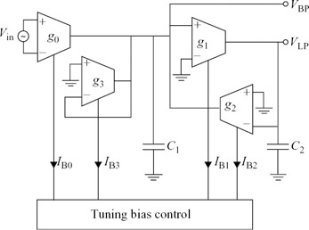
Figure 6.28: Tuneable OTA-C biquad
In the case where all components are ideal, the transfer function of Figure 6.28 is
![]()
By equating coefficients with the standard form of the second-order bandpass transfer function
![]()
we have
![]()
Suppose processing variations cause the transconductances of the OTA to vary. Because of the inherent matching between the components making up the OTAs, all transconductances will change by the same factor kg. Similarly, process variations will cause all the capacitor values to change by a factor kc, which in general will be different from, and unrelated to, kg. Including the factors kg and kc in (6.17) gives a new transfer function:
![]()
ω0 has been changed by a factor kg/kc. In order to restore the design value of ω0, the four OTAs are simultaneously tuned until kg = kc, in which case (6.20) reduces to (6.17). In practice, this is achieved by tuning the transconductances until ω0 is equal to the design value. It is also possible to tune Q independently of ω0 by varying g3 alone. However, because Q is determined by the relatively accurately defined ratios of C1 to C2, and g1, g2 to g3, it would appear that Q would remain virtually constant during the tuning process.
In a real design, however, circuit parasitics can have a major effect on the Q of the circuit of Figure 6.28. An ideal OTA has transconductance that is independent of frequency, but real OTAs have finite bandwidth, caused by parasitic high-frequency poles and zeros associated with circuit nodes inside the OTA. Although these normally occur far above the passband frequency of the filter, and have little effect on the magnitude of integrator gain within the passband of the filter, they increase the phase shift of the integrators to slightly more than the nominal 90 . This ‘excess phase’, as illustrated in Figure 6.29b, can substantially alter circuit Q.
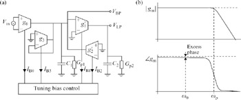
Figure 6.29: (a) Non-ideal biquad and (b) excess phase
In the frequency range of interest, where ω << ωp, the frequency-dependent OTA gain g′(s) can be modelled as an ideal transconductance g with an added phase shift proportional to frequency:
![]()
In the circuit of Figure 6.29a, the most significant influence of excess phase occurs in the two integrators made up of g1, C2 and g2, C1. Substituting this frequency dependent transconductance for the ideal transconductors in (6.17) and making appropriate approximations for ω0 << ωp gives a new value of Q for the circuit when excess phase is included:
![]()
Q′ is significantly affected by quite small values of excess phase. For example, if the design value of Q is 10 and ωp = 100ω0, giving rise to excess phase of about 0.6 , Q′ from (6.22) is 12.5, an increase of 25 per cent. A design Q of 50 will result in Q′ approaching infinity, and instability.
Another parasitic effect that modifies Q is the finite output conductance of OTAs. The output of an ideal OTA behaves as a current source, but real OTAs have significant output resistance. This can be modelled by conductances Gp1 and Gp2 shunting each internal circuit node to ground, as shown in Figure 6.29a. The transfer function of this modified circuit is given by:
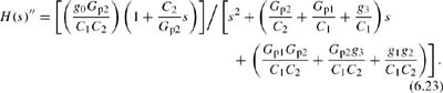
The Q of the modified circuit is approximated by:
![]()
Thus, increasing output conductance of the OTAs reduces Q. This sets an upper limit to the Q which can be achieved for a given set of transconductors and capacitors; as the design Q in (6.19) tends to infinity, the maximum achievable Q′′ is
![]()
In summary, the large tolerances of integrated components give rise to large frequency errors in the filter response, so integrated filters almost always require on-chip tuning. Frequency tuning will often be sufficient for filters operating at modest values of Q and frequency, typically lowpass and bandpass filters where the bandwidth is of the same order as the centre frequency. However in high-Q, high-frequency filters, circuit parasitics, principally the excess phase and finite DC gain of the active circuits, profoundly affect the Q of the filter response, so that Q must be tuned also.
6.4.2 On-line and off-line tuning
The outline of a typical tuning system is shown in Figure 6.30. A well-defined reference signal is applied to the filter input. One or more parameters of the filter output signal are measured by the frequency tuning control circuit and compared to a reference. The resultant error signal is used by the control circuit to calculate a correction signal, which is then applied to the frequency tuning input of the filter. Thus the system forms a closed feedback loop in which the filter is forced to converge on the desired frequency response. In a similar way, if implemented, the Q control circuit generates a tuning signal that corrects the Q of the filter.
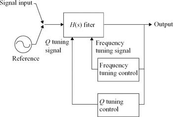
Figure 6.30: Outline of on-chip tuning scheme
Desirable features of any on-chip tuning system are minimal chip area and low power consumption. This requires simple hardware, and minimal computation requirements for the tuning algorithm. Conversely, the functional requirements placed on the filter design may be very complex, requiring several different performance goals for cut-off frequencies, gain, group delay, etc., which must be simultaneously met. It is not usually possible for an on-chip tuning system to evaluate all the relevant parameters of filter performance since this requires many measurements to be performed on the filter output signal over a range of frequencies. In high-order filters, there are many tuneable components, so achieving the desired filter response requires the control of a large number of variables simultaneously. For these reasons it is very difficult to directly tune a high-order filter using reasonably simple tuning circuits.
In order for the filter to function correctly, the tuning system must operate when the chip is first powered on. Also, component values will continuously drift while the circuit is powered, due to changes in environmental and operating conditions, so it is necessary to periodically repeat the tuning process during normal operation. This creates a problem in that the reference will be present within the filter passband at the same time as the desired signal, with the inevitable possibility of mutual interference occurring between the tuning system and the rest of the transceiver signal processing. The scheme of Figure 6.30 is therefore normally operated as an ‘off-line’ tuning system; periodically the normal signal input to the filter is removed, and the reference signal applied. The filter is then tuned, and the updated values of frequency and Q tuning signals stored until the next tuning cycle occurs.
These off-line tuning cycles can readily be accommodated in many transceiver architectures; for example, many transceivers alternate between transmit and receive; receiver filter tuning can take place during the transmit periods without affecting receiver operation. However, the additional signal routing and the requirement to store the tuning signals while the filter is on-line lead to added complication. Therefore, ‘on-line’ tuning is widely used where the tuning process proceeds continuously, and simultaneously with normal circuit operation. One way of achieving this is to devise a reference signal that has minimal effect on subsequent signal processing, but which at the same time can be used to measure the necessary filter parameters. An example of this is described in [30], where the reference signal is made nearly orthogonal to the received signal using spread-spectrum techniques.
6.4.3 Master–slave tuning
A very widely used and important on-line tuning scheme is the master–slave tuning scheme outlined in Figure 6.31. This makes use of the inherent good matching between components and circuit subsystems that are achieved within a single IC. Two well-matched filter sections are used; the reference signal is applied to the master section, whilst the actual input signal is applied to the slave section. The tuning system develops tuning signals in a closed feedback loop which correct errors in the response of the master section, as in off-line tuning. The same tuning signals are simultaneously applied to the slave section. If the master and slave sections are identical and perfectly matched, the response of the slave filter will be the same as the master. Thus it is unnecessary to apply the reference signal to the master filter, which can operate continuously.
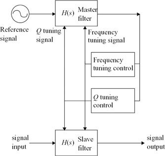
Figure 6.31: Master–slave tuning scheme
In practice, master and slave are usually different. The master section is usually a low-order filter, often a biquad, since this has a simple response for which it is relatively easy to design tuning algorithms and is economical of chip area and power consumption. This is illustrated in Figure 6.32; the master filter is a single biquad with a single resonance peak in its response. The slave section can be of whatever order is required to meet the filter specifications, with the same tuning signals applied to each section. The diagram shows the effect on the frequency responses of master and slave as they are simultaneously tuned. Clearly, it is much easier to design a tuning algorithm for the single biquad master when compared to the high-order slave response, with its multiple maxima and minima. Thus in addition to allowing on-line tuning, the master–slave tuning scheme provides a solution to the problem of tuning complex filters. A large proportion of high-order integrated filter designs therefore utilise master–slave tuning in some form.
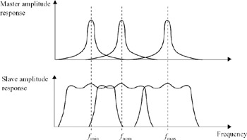
Figure 6.32: Tuning range of master and slave filter sections
The essential assumption made in the master–slave scheme is that the ratios of components in the master and slave sections can be accurately achieved, and will track each other precisely as the master section is tuned. If this is the case, the cut-off frequencies and Q of all the filter sections in the slave will exactly track those of the master, and if the master section Q is maintained at the correct value, the slave filter response shape will remain correct as the filter frequency is tuned. There are practical limitations on how nearly this can be achieved, and a substantial amount of design and layout effort must be expended to ensure that the master accurately models the tuning behaviour of the slave. Since parasitic effects can substantially alter the performance of the filter, these must also be accurately modelled in the master section. These requirements can usually be best met by designing the slave filter with circuits that are as near identical to the master as possible, and by making the tuning reference signal frequency close to that of the signal frequency. This allows the best matching between sections, and also ensures that frequency-dependent parasitic effects are similar in master and slave. Synthesis techniques are required that result in filter circuits using the minimum possible spread of component values.
6.4.4 Frequency tuning methods
For frequency tuning, the most commonly used input reference signal is derived from a stable clock oscillator. This is convenient, since most systems already include an accurate off-chip clock signal, usually derived from a quartz crystal, from which all on-chip clock signals are derived through various forms of frequency synthesis. At the output of the filter, phase comparison is the most widely used method of determining the state of tuning of the filter. An outline frequency tuning scheme is shown in Figure 6.33.
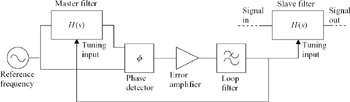
Figure 6.33: Outline frequency tuning scheme
In second-order filter sections, the phase difference between filter input and output reach well-defined values at the resonance frequency; 90 in the case of a lowpass section, 0 for a bandpass section. Accurate reference phase shifts independent of component value tolerances can be generated using digital counters operating on multiples of the reference frequency. An example of a phase detector is an analogue multiplier or mixer. With two inputs of the same frequency applied to the inputs, a DC output voltage is generated which is a function of the phase difference of the input signals. This transfer function is non-linear, and also depends on the signal amplitudes; but if the phase difference is arranged to be 90 , the output will be zero. Therefore, if the output of the phase detector is applied to the frequency tuning input of the filter via an error amplifier and loop filter, feedback around the loop will cause the cut-off frequency of the filter to reach a value giving the desired value of phase shift.
This system is, however, subject to several sources of error. With large initial errors in filter resonant frequency, the reference signal is likely to be outside the filter passband at the start of the tuning procedure. A filter section with high Q and therefore rapid cut-off in amplitude will attenuate the reference signal to a low level that may prevent the correct operation of the phase detector. This limits the scheme to low-Q filter sections. A low-Q filter has a phase response that changes only slowly as the frequency is tuned, therefore for a given tuning error, only a relatively small error signal is produced at the phase detector output. Therefore the signal-to-noise ratio inside the tuning loop is poor; small errors due to DC offsets in the phase detector, or parasitic phase shifts, give rise to large tuning errors. A further source of errors is distortion in the reference or filter output waveforms; applying a non-sinusoidal signal to the phase detector may result in incorrect output.
A modification of this method that avoids these problems is to replace the filter section being tuned by a voltage controlled oscillator (VCO). This can be achieved by applying feedback with the appropriate gain and phase to the filter section. Oscillation then occurs at the resonant frequency of the filter. The output signal frequency is compared with the reference frequency using a phase detector, and the error signal is used to tune the VCO as before. This system is therefore a phase-locked loop, as shown in Figure 6.34. The advantage of using the output frequency of a VCO rather than the phase shift through the filter section as the basis for tuning is that the system is independent of fixed errors in the phase comparison; provided the phase difference between reference and VCO is maintained constant, the VCO frequency, and therefore the resonant frequency of the filter, is identical to the reference.
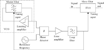
Figure 6.34: PLL frequency tuning system
The main source of tuning error in this system is the mismatch in behaviour between the filter section, operating at finite Q and with relatively low signal levels, and the VCO which effectively operates at infinite Q and inherently requires a nonlinear amplitude limiting mechanism to achieve a stable signal amplitude. To ensure that the frequency-determining elements operate within their linear range, the VCO is usually implemented by adding a limiting amplifier to provide feedback around a bandpass biquad filter section.
Many successful frequency tuning systems using frequency- or phase-locked loops as described have been implemented in practical designs, for example References 31 and 32. These methods are well suited to master–slave designs, where the tuning loop can operate continuously. This yields an extremely simple control system, and is often capable of frequency tuning accuracy within 1 per cent. These techniques become increasingly difficult to apply at the highest frequencies, due to the increasingly severe errors caused by excess phase, both in the filter or VCO and in the phase detector itself.
Frequency tuning techniques can utilise the time-domain response of the filter. The response of a high Q bandpass filter to a step or impulse function is a damped sinusoid at the filter output. The period of the sinusoid is approximately related to the resonant frequency of the filter. The filter output waveform is squared using a limiting amplifier, and the period measured using digital counter techniques. A tuning signal is derived by comparing the measured period with the desired value. In order to achieve good accuracy, high resolution in the period measurement is necessary. This requires that the transient response has a long duration. The duration increases with Q and filter order, and due to this and the iterative nature of the measurement technique it is most appropriate for off-line tuning of high-order, high-Q bandpass filters [33, 34]. This tuning control method is digital in nature, so is easily combined with switched array tuning schemes.
A related technique is to measure the time constant of an integrator using a DC charging current. An example of this technique using an OTA-C integrator is shown in Figure 6.35.
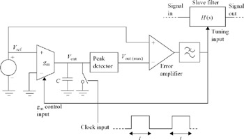
Figure 6.35: Frequency tuning scheme based on ramp generator
An accurate clock signal is used to open the switch for a period t. During t, the integrator output voltage is a linear ramp that reaches a maximum value of
![]()
This maximum voltage is stored by the peak detector, and compared with the reference voltage by the error amplifier. The resulting low-pass filtered error signal is applied to the OTA transconductance control input and causes the capacitor charging current and therefore Vout(max) to vary. Over a large number of clock cycles, this feedback loop causes Vout(max) to become equal to Vref:
![]()
Since t is accurately defined by the clock signal, and the resonant frequency of the filter is accurately proportional to gm/C due to well-defined ratios between all transconductances and capacitances on the chip, the resonant frequency is set to the correct value.
In order to avoid problems caused by unwanted phase shifts, frequency tuning methods have been devised based on amplitude measurements. A second-order response with Q greater than 1/√2 contains a peak in its amplitude response plotted against frequency. For high Q values, the amplitude peak closely approximates the resonant frequency. Tuning the resonant frequency of the filter with a fixed input reference frequency will also produce a peak in output response when the two frequencies coincide. The tuning system only needs to detect when the maximum output signal is achieved; the amplitude detector need therefore have neither high accuracy nor linearity, provided it has a monotonic response.
A tuning scheme using this principle is shown in Figure 6.36. The reference signal is applied to the biquad input, and the envelope detector produces a DC level, Venv, proportional to the amplitude of the filter output. In the first phase of the tuning cycle, the filter tuning voltage Vtune is swept through its range by the ramp generator. At the point where the resonant frequency of the filter coincides with the reference frequency, the filter output amplitude and thus Venv reaches a maximum, and this value is stored by the peak detector as Vpk. In the second tuning phase, Vtune is swept again, and Venv is compared with Vpk by the comparator. At the point where the resonant frequency and reference frequency coincide, Venv is equal to Vpk and the control logic opens the switch. Thus the value of Vtune giving the correct filter resonant frequency is stored on the hold capacitor, until the next tuning cycle begins.
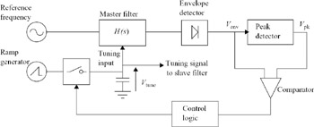
Figure 6.36: Frequency tuning based on amplitude peak detection
In practice, the circuit of Figure 6.36 will suffer tuning errors due to parasitic charge injection and loss from the tuning voltage holding capacitor, and offsets in the comparator and peak detector. However, a more sophisticated implementation of this technique has been described [35] in which these errors are largely eliminated.
6.4.5 Q tuning techniques
Frequency tuning ensures that the centre frequency or cut-off frequency of the filter is tuned to the correct value; however this does not necessarily ensure that the shape of the frequency response is correct; this also depends on the Q of the filter sections. As noted above, parasitic effects in particular may lead to severe distortion of the filter response. The frequency tuning schemes described above are independent of Q. However, in order to tune the filter Q, it is first necessary that the frequency tuning process is completed, because Q is defined in terms of the way that filter response changes close to the resonant frequency. Any error in the filter resonant frequency will therefore also result in errors in Q. A further difficulty is that although the designer will attempt as far as possible to make Q unaffected by frequency tuning and vice versa, they are never entirely independent. Inevitably, tuning Q will introduce a new error in filter frequency, and correcting this error will alter Q again.
Therefore, several iterations of frequency and Q tuning may be required to correctly tune the filter, or the two processes must proceed simultaneously. The designer must take the interdependence of both tuning processes into account in order to ensure that convergence takes place [36]. This is especially difficult with high-Q filter sections, where as seen in Section 6.4.1, Q is sensitive to small changes in tuning, and instability can easily occur.
The most widely used Q tuning technique [35, 37] utilises the fact that in many cases the gain of a biquad at the resonant frequency is proportional to the Q. For example, in the case of the OTA-C biquad of Figure 6.16, from equations (6.12), (6.13) and (6.14), we can derive expressions for the gain in terms of Q at ω0:
![]()
The Q-tuning system of Figure 6.37 is an amplitude locked loop which operates using this proportionality between gain and Q. It is assumed that separate frequency-tuning circuits maintain ω0 of the filter exactly equal to the desired value, and that the gain of the filter is equal to the Q at ω0. The reference signal is attenuated by a factor 1/KQ by a potential divider, and applied to the filter input. The output amplitude of the filter is therefore Vref Q/KQ. A pair of matched envelope detectors generate DC levels proportional to Vref and the filter output, which are compared by an error amplifier. The resulting feedback signal varies the Q of the filter so that the filter output is equal to Vref, in which case Q = KQ. Since KQ is determined by component ratios which can be made accurately, Q is also accurately defined.
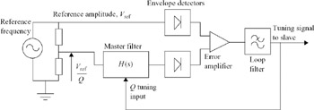
Figure 6.37: Q tuning scheme
6.4.6 Tuning of high-order leap-frog filters
Multiple loop feedback filters are desirable for fully integrated filters because of their low sensitivity. This applies especially to high-Q bandpass filters, due to their high sensitivity to frequency tuning errors, and the high Q required from each filter section. However, as pointed out in Section 6.3, the multiple feedback structure which is responsible for this low sensitivity at the same time makes this type of filter more difficult to tune. One method of overcoming this difficulty is to use master– slave tuning systems; however in the case of high-Q bandpass filters, it may not be possible to ensure sufficiently accurate matching between sections of the filter circuit to obtain adequate tuning accuracy. This section describes a tuning method applicable to the leapfrog (LF) form of MLF filter, and other types of filter based on LC ladder simulation, in which the individual pole frequencies are tuned without relying on precise matching [38].
The same tuning problem exists when tuning passive LC bandpass filters, such as the ladder filter shown in Figure 6.38. Synthesis of this ladder filter with centre frequency ω0 results in the inductor and capacitor values in each branch of the ladder having the same resonant frequency, 1/LiCi = ω20. One method of tuning the filter would be to isolate each ladder branch, resulting in several separate second-order bandpass sections, which could then be individually tuned to the correct centre frequency. The drawback of this approach is that considerable additional circuitry would be required to route the test signal to and from each resonator in turn. This routing circuitry would also introduce additional parasitic capacitance and cross-talk between filter sections, degrading filter performance. An alternative method of tuning this filter which avoids some of these problems is due to M. Dishal [39]. This has been widely applied to many forms of passive bandpass filter. It has the advantage of requiring no additional signal paths connected to the internal nodes of the filter.
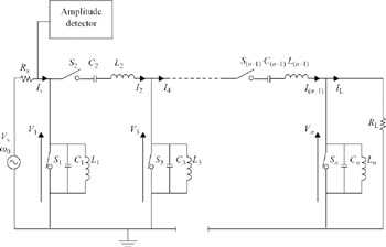
Figure 6.38: LC bandpass tuning using Dishal's method
To tune the filter of Figure 6.38, initially all switches in the series arms are open, and all those in the shunt arms are closed. A signal is applied to the input at frequency ω0, and V1 is monitored by the amplitude detector. S1 is opened, and C1/L1 are tuned to parallel resonance, i.e. maximum amplitude of V1. Since S2 is open, the resonator C1/L1 is isolated from the rest of the circuit, which therefore does not alter the resonant frequency. Next, S2 is closed, and C2/L2 are tuned to series resonance and minimum V1. Since S3 is closed, C2/L2 are also isolated from succeeding stages of the filter. Each successive branch is then adjusted in turn, the shunt branches for maximum V1 and the series branches for minimum V1, with the associated switch being opened or closed. Since all preceding branches are already resonant, the reactive component of their net series or shunt impedance is zero, and they are ‘transparent’ at frequency ω0. When Ln/Cn have been adjusted, the tuning process is complete. In tuning schemes for second-order cascade filters, it is normally necessary to provide Q-tuning capability. This is not done when tuning using Dishal's method as described, and so the tuning process does not completely define the transfer function of the filter. The bandwidth and ripple in the response are defined by ratios between component values in different branches of the circuit, whilst the method described above only tunes the inductor and capacitor in each individual branch in isolation. However, because all branches are resonant at ω0, the passband is symmetrical, insertion loss is minimised, and gross distortion of the frequency response does not occur.
As discussed in Section 6.3, a widely used technique for active filter design is to simulate the function of passive LC ladder filters using active elements. Two methods for doing this are the component substitution technique, and the leap-frog MLF filter. Clearly, using the component substitution technique, the inductors of Figure 6.38 could be replaced by gyrators which performed the same circuit function, and Dishal's method could still be applied to tune the circuit. A leap-frog MLF filter which simulates the filter of Figure 6.38 is shown in Figure 6.39. In this structure, the reactive passive components are replaced by integrators.
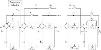
Figure 6.39: LF simulation of LC bandpass filter
Examination of this block diagram shows that each LC resonator in the prototype is replaced by a two-integrator loop bandpass biquad of the type shown in Figure 6.5, with the same resonant frequency, ω0, and transfer function of the isolated LC circuit. As in the case of the LC bandpass filter, it would be possible to tune each resonator separately, as is proposed in Reference 40, but with the same drawbacks with regard to signal routing. In the LC filter, coupling between resonators occurs because of their ladder connection; in the LF filter, this coupling occurs via the feedback paths. The switches in the feedback paths of Figure 6.39 perform an equivalent function as in Figure 6.38, isolating the resonators from one another. Dishal's method can therefore be applied to the MLF filter, tuning the resonant frequency of each biquad in turn for alternate maximum or minimum amplitude at V1, the output of the first integrator. V1 is analogous to the voltage at the input termination of the ladder filter prototype.
An on-chip tuning system which tunes the pole frequency of a single biquad by detecting the peak of its amplitude response is described in Section 6.4.4. This scheme may be extended as in Figure 6.40 to sequentially tune a number of biquads making up the bandpass LF filter. Initially, Vtune1 is adjusted for peak output at V1. To isolate the first biquad from the rest of the filter, Vtune2 …, VtuneN are initialised to zero, debiasing the other biquads. After Vtune1 has been adjusted, Vtune2 is tuned for minimum V1. The minimum detector is a peak detector with inverted polarity. The process is repeated with Vtune3,…, VtuneN until all biquads have been tuned.
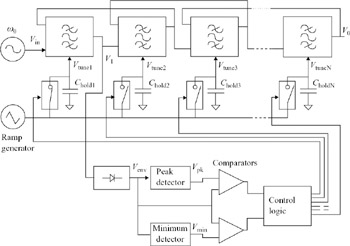
Figure 6.40: Peak-detecting tuning scheme extended to LF bandpass filter
|
EAN: 2147483647
Pages: 100