Carbon Nanotubes
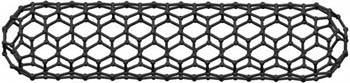
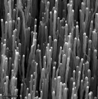
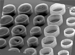
| Brent Segal Since their discovery in 1991 by Sumio Iijima, carbon nanotubes have fascinated scientists with their extraordinary properties.[1] Carbon nanotubes are often described as a graphene sheet rolled up into the shape of cylinder. To be precise, they are graphene cylinders about 12nm in diameter and capped with end-containing pentagonal rings. One would imagine that a new chemical such as this would be discovered by a chemist, slaving away in front of a series of Bunsen burners and highly reactive chemicals, with a sudden epiphany being revealed in a flurry of smoke or precipitation from a bubbling flask. However, carbon nanotubes were discovered by an electron microscopist while examining deposits on the surface of a cathode; he was performing experiments involving the production of fullerenes, or buckyballs. This discovery presents one of the key tenets of nanotechnology. Novel tools allow researchers to observe materials and properties at the nanoscale that often have existed for hundreds or thousands of years and to exploit the properties of such materials. After Iijima's fantastic discovery, various methods were exploited to produce carbon nanotubes in sufficient quantities to be further studied. Some of the methods included arc discharge, laser ablation, and chemical vapor deposition (CVD).[2] The general principle of nanotube growth involves producing reactive carbon atoms at a very high temperature; these atoms then accumulate in regular patterns on the surface of metal particles that stabilize the formation of the fullerenes, resulting in a long chain of assembled carbon atoms. The arc-discharge methodology produced large quantities of multiwalled nanotubes (MWNTs), typically greater than 5nm in diameter, which have multiple carbon shells in a structure resembling that of a Russian doll. In recent years, single-walled nanotubes (SWNTs) using this method also have been grown and have become available in large quantities. The laser ablation method of carbon nanotube growth produced SWNTs of excellent quality but requires high-powered lasers while producing small quantities of material. The CVD method was pioneered by Nobel Laureate Richard Smalley and colleagues at Rice University, whose experience with fullerenes is nothing short of legendary. This growth technique is aided by a wealth of well-known inorganic chemicals specifically involving the formation of highly efficient catalysts of transition metals to produce primarily single-walled nanotubes. Figure 13-2 shows a simple carbon nanotube. Figure 13-2. A simple example of a carbon nanotube. (Courtesy of Dr. Peter Burke, University of California, Irvine.) Novel PropertiesAlthough carbon nanotubes have a suitably interesting structure, there are a multitude of important properties that impart the potential for novel applications of significant commercial value. Multiwalled and single-walled nanotubes have similar properties, and for illustration, focusing on single-walled nanotubes provides a reasonable primer of the primary features. Some of these properties include remarkable strength, high elasticity, and large thermal conductivity and current density. Several reports have determined that SWNTs have a strength of between 50 and 100 times that of steel.[3] The elasticity of SWNT is 11.2 terrapascal (TPa), a measure of the ability of a material to return to its original form after being deformed. Imagine a molecule that, on the atomic scale, is as strong as steel but flexible like a rubber band! Despite these structural properties, SWNTs have a thermal conductivity almost as great as twice that of diamond, which is known to be one of the best conductors of heat. Perhaps one of the most impressive properties of SWNTs involves their electrical conductivity, which is reported to be 109 Amps per square centimeter, which is about 100 times that reported in copper, the conductor of choice for nearly every electrical device in common use today. SWNTs have two types of structural forms, which impart an additional set of electrical characteristics. Depending upon the alignment of the carbon atoms in the cylindrical form, SWNTs can be either achiral (having atomic uniformity along its axis) or chiral (having a twisted alignment from the uniform case). Achiral and chiral forms can act as metals or semiconductors and yet retain the same basic nanotube structural motif. In addition to these well-known properties, SWNTs have other features that make them attractive beyond their scientific novelty. SWNTs have a density approximately half that of aluminum, making them an extremely light material. SWNTs are stable at temperatures up to 2700°C under vacuum. This is truly impressive considering the melting point of Ruthenium, Iridium, and Niobium metals are about the same temperature.[4] Although nanotubes have structural uniformity, the carbon atoms within them have the same precise features as a typical graphene sheet. These atoms can be derivitized to alter the structure of the SWNTs, allowing their properties to be tailored. This allows nanotubes to be subject to literally hundreds of years of rich organic chemistry. Carbon nanotubes not only can be functionalized to change their structure but also can interact beneficially with organic chemicals that have biological usefulness. Fullerene materials have been explored for use as antioxidants, drug-delivery agents, and amino acid replacements; the latter could lead to new drug candidates. Reports have been published of their benefits in enhancing virus-specific antibody responses or as a scaffold for growing retinal epithelial cells to be transplanted into the retina to treat macular degeneration.[5] Manufacturing and Scaling IssuesCarbon nanotube synthesis in recent years has been driven by yields and cost. To move nanotubes from scientific curiosity to practicality, they must be available in sufficient quantities at a reasonable cost with high uniformity and reproducibility. In the case of MWNTs, the arc-discharge method provides a good alternative, yielding large quantities of material at a good cost. In the case of SWNTs, while generating large quantities of material, the purity is often unacceptable for a subset of applications because of excessive carbonaceous contamination. Instead, the CVD method and a recent alternative, plasma-enhanced chemical vapor deposition (PECVD), have burst onto the scene as the methods of choice for producing large quantities of SWNTs with micron lengths, purity, and reliability within specifications for certain applications. Figure 13-3 shows an example of PECVD nanotubes. Figure 13-3. Array of carbon nanotubes grown by plasma-enhanced chemical vapor deposition. PECVD has been reported to lower the temperature of nanotube growth significantly by using a plasma to generate the reactive carbon atoms instead of very high temperatures, as in standard CVD growth. In the case of nanoelectronicsperhaps one of the early applications for which SWNTs will be adoptedextremely high purity nanotubes are required, and only a few providers have managed to generate such materials at a reasonable cost. The key issue with respect to commercial use of nanotubes for most applications comes in placing wafers on silicon or silicon on insulators, which are typical substrates for making circuits or devices. To the extent that alignment or specific orientation is required, applicability has been limited. Two general methodologies exist for proceeding toward manufacturability of devices: specific growth using prepatterned catalysts (Figure 13-4), or patterning of nonoriented fabrics using application of solutions. In the former case catalysts are placed in specific regions of a substrate onto which nanotubes grow in either a vertical or a horizontal direction. Figure 13-4. Patterned growth of multiwalled carbon nanotubes by chemical vapor deposition. Vertically oriented growth has been demonstrated by several groups and is especially valuable for field emitting devices. Many potential CNT device approaches using CVD growth of SWNTs suffer from manufacturability and scalability issues, primarily because typical CVD temperatures are >800°C for SWNTs. At such high temperatures, other steps in a fabrication process can be adversely affected, causing the yields of working devices to be lower. Indeed this a serious limitation if the underlying substrate or control electronics cannot withstand such temperatures. Some reports have presented data on lower-temperature methods of growing SWNTs using techniques such as PECVD. These techniques are still in their infancy but could represent a reasonable pathway for certain types of devices or applications. Horizontal fabrics have been applied to substrates whose thickness can be controlled by solution concentration and application procedure. Such methods have conquered the issues of purification of nanotube solutions, distribution of networks of nanotubes of uniform density over large substrates, and patterning of traces of conductive nanotubes into shapes that can be further integrated into complicated process flows. SWNTs can be obtained in bulk from various suppliers, which have exploited advanced CVD techniques to grow SWNTs in large scale of excellent quality. These nanotubes can then be purified to remove metallic contaminants (for example, Group IA and IIA elements) used in the growth process and carbonaceous species that serve as a potential source of contamination. The processed SWNTs are solubilized and can then be applied to device substrates for further processing. Potential ApplicationsA variety of potential applications exist for carbon nanotubes. MWNTs have been reported for use primarily as a composite for batteries and as field emitters for television monitors.[6] As the price for these materials continues to drop, other potential applications, especially as additives in composites, are likely. The molecular nature of carbon nanotube fabrics allows various CNT physical properties, including electromagnetic, mechanical, chemical, and optical behaviors, to be exploited to create integrated electronic devices (including nonvolatile memory devices); chemical, biological, and radiation sensors; passive low-resistance, low-capacitance conformal interconnects; and electromagnetic field emission devices, scaffolds for cell growth, antioxidants, and near infrared imaging tags for biological samples and cells, to name a few. Table 13-1 summarizes a number of proposed applications that could use SWNT fabrics as an enabling component.[7]
One existing application for which SWNTs are particularly useful is in the arena of electronics, specifically to create nonvolatile memory.[8] In the case of nonvolatile memory applications, significant progress has been made in using fabrics, or assemblages of SWNTs, as electrical traces within integrated circuits.[9] These fabrics retain their molecular-level properties while eliminating the need for nanoscale physical control. These monolayers are created by room-temperature spin-coating of a solution of SWNTs in a semiconductor-grade solvent. After evaporation of the solvent, the resulting monolayer fabric is lithographically patterned and etched in an oxygen plasma. The process of spin-coating SWNT solutions can be used to produce monolayer fabric of very steep aspect ratios, which allows coverage of fabrics over sharp edges or tall structures. Such diversity in the coating of nanotube fabrics on three-dimensional structures has the potential to support traditional horizontal integration schemes in electronics as well as a novel set of devices oriented in a vertical fashion that could lead to significantly more dense electronics. The combination of patterned nanotube fabrics and the use of fabricated sacrificial layers around the fabric allows the formation of an open cavity, in which a suspended patch of fabric can be mechanically drawn into electrical contact with an electrode. These devices, called molecular microswitches (MMSs), can be used as storage elements for memory or logic applications. The SWNT fabric approach uses a 12-nm thick patterned SWNT fabric and can be interconnected monolithically with additional standard semiconductor (for example, CMOS) circuitry above or below, providing buffering and drive circuitry to address and control the MMS devices. When this technique is used, the limit to the scalability of the hybrid nanotube/ CMOS system depends only on the available photolithographic node. Hence, the CMOS fabrication, and not the inclusion of nanotubes, remains the limiting factor in scaling. Indeed, the ultimate physical limit to the integration density of this approach scales down to two individual metallic nanotubes and their electromechanical interaction. |
EAN: 2147483647
Pages: 204