2.1 Computer Structures
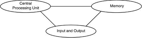
| Nearly all microcomputers share the same overall structure, consisting of three essential components that are visible to the assembly language programmer:
These components must be interconnected in some fashion, as indicated schematically in Figure 2-1. In a typical implementation of any architecture, the interconnections take the form of a bus, or several buses, to convey control signals and data. Think of a bus as a band of parallel wires, with each wire dedicated to carrying one bit of data or one particular control signal. Greater bus width tends to correlate with increasing both cost and overall performance. For example, IBM designed the first PC around the Intel 8088, which has a 16-bit core but an 8-bit external data bus. The other alternative was the Intel 8086, which has a 16-bit data bus as well as a 16-bit CPU, and would have offered greater performance at greater expense. Figure 2-1. Basic computer structure
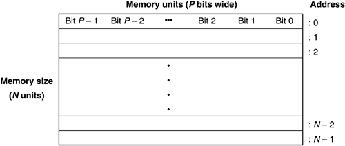
2.1.1 The Central Processing UnitThe central processing unit (CPU) is the brain of the computer, and its activities are paced by a high-speed heartbeat in the form of signals from an oscillator (clock). The CPU fetches instructions and data from, and stores data into, chosen memory cells. The CPU then executes the fetched instructions, performing whatever arithmetic and logic operations are specified by those instructions. The CPU can manipulate addresses (i.e., pointers to data) as well as data. In addition, the CPU can redirect program flow along different paths according to the values of computed intermediate results. Finally, the CPU can execute instructions that initiate input and output with peripheral devices. A central processing unit contains circuitry for internal control (control path) and circuitry for actual computation (datapath, sometimes written as data path). The datapath is usually considered to comprise one or more arithmetic and logic units that perform computation, an array of processor registers, and interconnections for the flow of information among these parts. The registers internal to the CPU provide local, high-speed storage for the processor. These registers can hold either data or memory addresses. Some computers have general-purpose registers that can be used for any function, while others have distinct sets of registers to perform different functions. Since register storage within the CPU offers the fastest possible times for access to computed data, we have seen a clear historical trend towards more and more registers, as indicated in Tables 1-3, 1-4, and 1-5. Itanium architecture specifies several types of registers: 128 integer registers used for addresses or integer data, 128 floating-point registers, and additional groups of specialized registers. Such CPU registers and their width in bits are visible to the assembly language programmer (Table 1-5). Indeed, assembly language programming intrinsically involves register-level programming; registers are not normally accessible to the high-level language programmer. The specialized instruction pointer (IP) register of an Itanium processor contains the address of the next instruction to be fetched. The register with this same function in many other architectural families is known as the program counter (PC). 2.1.2 The MemoryThe memory of a computer serves as its main information repository. Almost from the beginning of the development of computer architectures, a single memory structure has been used to hold both instructions and data, as proposed by John von Neumann (1903 1957). Over time, many types of physical components have been employed as memory elements. Nearly all of these from magnetic cores to semiconductor circuit elements (flip-flops and latches) are based on some physical two-state property. Therefore each fundamental unit of memory storage represents one binary digit, or bit. Bits in memory are arranged as an array of information units, with each unit composed of a fixed number of bits, as shown in Figure 2-2. All memory structures share two organizational features:
Figure 2-2. Memory organization
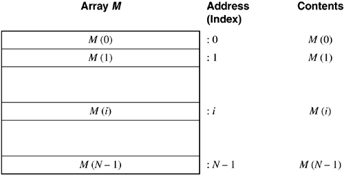
At the architectural level, it is essential to distinguish between two aspects associated with each information unit:
The address of a particular information unit never changes, but its contents may be highly volatile. Figure 2-3 shows another view of memory, as a large one-dimensional array, M(), where each element of the array contains one unit of information. The index, i, is the address of a unit; using that address we can locate the contents of the particular unit, M(i). Figure 2-3. Memory as an array
In the past, different computer architectures specified various values for the word size P, which is the number of bits for each information unit. Larger word sizes were thought to accommodate the needs of scientific calculations. The first minicomputers specified word sizes as small as one byte (8 bits) for economy of design. Contemporary designs take another approach. At the architectural level, the memory is byte addressable. At the implementation level, the actual smallest amount of information stored or retrieved may be some multiple of a byte. The Itanium architecture enumerates memory addresses just as though the fundamental information unit were one byte in size. Certain machine instructions can specify the movement of 1, 2, 4, or 8 bytes of data between a register and memory. As we shall see, the larger selection of sizes for moving data makes working with different types of data representations more efficient. The address space is the set of all addresses, the collection of all distinct information units that a program can reference. The number of bits used to represent an address N determines the size 2N of the address space (Tables 1-3, 1-4, 1-5). Unless a computer system design provides for special hardware elements for extended addressing, an address is usually less than or equal to the maximum value 2N 1 allowed by word size or the datapath width for a given architecture. The era of 16-bit minicomputers ended when programmers began to have difficulty accommodating large data structures or solving complex problems using only 64 kibibytes of addressable memory (65,536 unique memory addresses). For quite a while thereafter, the 4-gibibyte address space of 32-bit architectures seemed ample for nearly all applications. Currently, the manipulation of large graphic and video files, the organization of data from satellite and astronomical observations, the extraction of patterns from genomics data, and the daily operation of many modern commercial database applications can all benefit from the 16-exbibyte address space (18,446,744,073,709,551,616 unique memory addresses) provided by 64-bit computer architectures. As CPU speeds have increased more quickly than memory access speeds, system designers have had to introduce cache memory in order to produce high-performance implementations for every contemporary computer architecture. A cache subsystem is composed of faster, but more expensive, memory components; it holds copies of instructions or data from frequently accessed memory locations. In some architectures, cache memory is an implementation feature that is invisible to an assembly language programmer (except indirectly through the perception of improved throughput). In other instances, such as the PowerPC® and Itanium architectures, the cache memory is an architectural element that the system or application programmer can control, to varying extents, using the machine's instruction set. The Itanium architecture provides for control of up to three levels of cache. 2.1.3 The Input/Output SystemVarious types of input/output (I/O) devices allow the processor to communicate with humans, with other processors, and with secondary storage devices that are slower than main memory but larger in capacity. These external devices may include displays, printers, scanners, network interfaces, disks, and audio hardware. Such devices are highly diverse in speed, amount of data transferred in a single operation, and degree of processor intervention required. Some operating systems attempt to bring most peripheral devices within a standardized protocol for setting up data transfers, while others may treat all terminals and printers in one way, all disks in another way, etc. These aspects of external devices, which lie outside the scope of this book, are often explored in books about operating systems. All but the simplest devices in the simplest computers are capable of moving data directly to and from memory after the processor has specified overall parameters, such as a starting memory location and a total amount of data to be moved. Special hardware devices called direct memory access (DMA) controllers allow such transfers to proceed in a time-overlapped fashion with other computing activity. The components of system software directly concerned with I/O are often called device drivers. Again, this book does not attempt to discuss device drivers in any detail, although we may note in passing that these are the operating system components that are most likely to be written in assembly language. A processor can communicate with I/O devices through special-purpose instructions and/or through some or all of the same machine instructions that move data between the CPU, its registers, and memory. Numerous early mini- and microcomputer architectures used the former strategy of special I/O instructions, such as IN and OUT for certain Intel architectures (Table 1-3). The family of Digital architectures that we discuss from time to time in this book use the latter memory-mapped I/O techniques through the regular instruction set (Table 1-4). In contemporary computer systems, most I/O devices are connected in the first instance to a high-performance bus (such as PCI), and that bus is connected through a bridge controller to the memory CPU bus. Ultimately, the I/O bus address space is made available to the processor and generally appears mapped into a virtual address space in a manner that does not conflict with the addressing of physical memory. An operating system can then use device drivers that communicate with peripheral devices by means of load and store instructions using those special addresses. |
EAN: N/A
Pages: 223