2.3 Distinguishing features of the mainframe
| Let us go deeper into the structure of three main resources defined by the S/360 architecture.[4] It is this structure and implementation that distinguishes the mainframe from other vendors' computer implementations and that can give some significant value to your business opportunity.
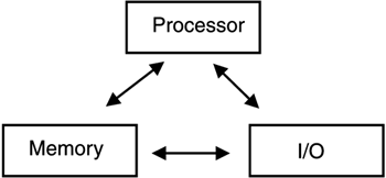
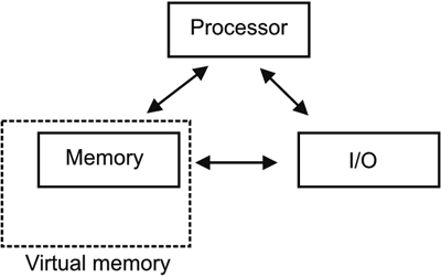
The mainframe is based on the von Neumann computer model (see Figure 2-3), with these main parts:
Figure 2-3. The von Neumann computer model
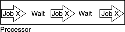
2.3.1 Central processing unitIn this section, we will take a look at how the architecture and design of the central processing unit (CPU) contributes to the reliability and scalability of the mainframe. The design aims to optimize the workloads that are run on the machine. Architecture of CPUThe architecture of the CPU defines data integrity and work separation. Data integrity means that an instruction either completes accurately or the reason for the error can be found. One instruction is executed at a time. If it does not complete, the architecture defines how this will be handled. In other words, the mainframe is self-checking. Work separation alludes to the fact that the CPU can run in either of two modes: supervisor (or privileged) mode and problem mode. The two states ensure that only properly authorized programs, like the operating system itself, can perform critical actions. At the same time, user programs can run without fear of their interfering with another program's or operating system's data. To protect data, storage protect keys were initially used. Later, technologies such as virtual memory and address spaces were developed. The mainframe architecture defines the order in which instructions are to be processed as "next sequential instruction" (NSI). However, in the mainframe design there are two exceptions to the sequential rule: branching and interrupts. When branching, the program branches to an address specified in a branching instruction instead of executing the next instruction as specified. Interrupts signal external events that have an impact on the sequence in which instructions are executed. A little known fact is that, statistically, every fifth instruction is a branch. So while the mainframe architecture defines it as an NSI machine, the CPU is designed around the fact that processing is constantly going down different paths. In the CPU design, a lot of effort has gone into ensuring that both branching and interrupts are handled as efficiently as possible. These efforts are ultimately the reason for the speed of processing. MultitaskingEarly systems processed work as it came in as a job unit. Each job was processed as a whole, and only one job was processed at a time. Jobs often had to wait (for example, for information from a printer or a tape drive), and the CPU was idle much of the time, as illustrated in Figure 2-4. The speed of the external devices was much slower than that of the CPU. Figure 2-4. An active job causes the CPU to be idle while the program is waiting for I/O
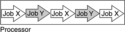
In contrast to a personal computer, a mainframe is designed to support many users at the same time. On a PC, you might not really care how busy the CPU is, because you are the only user on it. On the mainframe, thousands of different pieces of work compete for processing resources. Finding a way to keep the CPU working while a job waited would increase the amount of work the CPU could process. The solution was multitasking. Multitasking means that when a job waits for I/O, another job can be processed, as illustrated in Figure 2-5. Figure 2-5. Multitasking: While one job waits, another can be processed
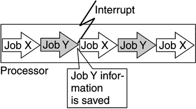
In order to implement multitasking, a technique was needed to switch control from one job to another. This switching is achieved by interrupts. An interrupt is an event that alters the sequence in which the CPU executes instructions, as illustrated in Figure 2-6. Figure 2-6. Interrupts alter the execution sequence of instructions
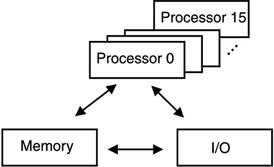
An interrupt can be planned (specifically requested by the program) or unplanned (caused by an event that is not related to the executing task). See Chapter 21, "Mainframe Reference" for more details on the interrupt technique. Interrupts and multitasking are possible because the relevant information about the interrupted program is captured and saved. This is called state handling and allows the CPU to continue executing a program where it left off. The interrupt technique enables a program to wait for work without consuming significant resources, as the program does not need to constantly check if there is work to be processed. Programs will be called by an interrupt when data for processing are available. MultiprocessingEven the most efficient CPU can execute only one instruction at a time. As the workload increases, thousands of jobs can wait for a single CPU. In this situation, it might make sense to add CPUs. Two or more CPUs processing simultaneously make up a multiprocessor. Multiprocessing on the mainframe was introduced with the S/370 architecture in 1970. Increasing the number of CPUs increases the demand on the operating system. Linux is an operating system that handles multiprocessors fairly well, as we shall see in Chapter 3, "Introducing Linux on the Mainframe." Today's mainframe (for example, the zSeries 900) is a Symmetric Multiprocessor (SMP)[6] with up to 16 CPUs as illustrated in Figure 2-7.
Figure 2-7. An SMP with 16 CPUs
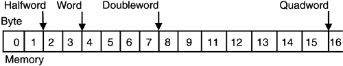
A mainframe CPU can sustain a utilization of over 90% over long periods of time. 2.3.2 MemoryMemory's task is to serve data to the outside world. Memory either receives data and stores data safely, or gives data out. Memory serves many masters, including the CPUs and the I/O subsystem. This being the case, memory is optimized to do its job quickly and provide for data integrity while doing it. The memory subsystem does multitasking and knows how to keep track of all the requests for data. For example, when a program tries to use data that it shouldn't, an interrupt occurs, and a program is brought in to handle the problem. Architecture of memoryInitially, the architecture defined a flat, real memory space. Memory was addressable by bytes, half words, full words, and double words (see Figure 2-8). Eventually, quadwords (4 words) and page were added for addressing, depending on the instruction or I/O operation being run. Figure 2-8. Memory can be visualized as a horizontal string starting at zero and extending to the limit of memory
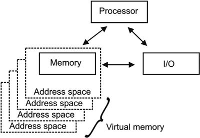
As CPU speed increased, it was only a matter of time before a CPU could execute more programs in a given period of time than it could hold in its own storage. Again, the CPU was idle for periods of time. The solution was to bring pieces of a program into memory (or real storage) instead of the entire program. The program pieces, called pages, were fixed in size (4 KB today). Each page was assigned a unique address defined by the first byte of the page. That address was called the virtual address. The CPU kept track of which pages were in real storage and which it would have to get by way of a table that listed the page addresses for the program that was executing. Thus, memory was no longer limited to the size of real storage, but to the number of virtual addresses (see Figure 2-9). Figure 2-9. Virtual memory lets programs address a virtual address range. Only a subset may be residing in real memory at any time.
The benefit which programmers see from virtual addressing is that the program is freed from the constraints of real memory. Programmers can still address memory as if it were a flat array. The operating system resolves the addressing at runtime by paging.[7]
Address spaces full range of memory, yet isolation guaranteedWhat is an address space on the mainframe? An address space is a range of contiguous virtual storage addresses that the operating system creates. A small portion of an address space is reserved for system data and programs, but most of an address space is available for user data and programs. The first version of IBM's OS operating system to use virtual memory, the Single Virtual Storage (SVS) system, removed the constraint on real storage and provided a single 16-megabyte virtual address space to be divided among all tasks. When more than one program is running on a computer, the issue of isolation becomes important. Programs must not be allowed to write into memory reserved by others. There are several techniques for doing this, including allocating a separate piece of real memory to every program. Real memory is divided into "n" pieces, plus an overhead for the operating system. Only six months after the release of SVS in 1972, the Multiple Virtual Storage (MVS) operating system introduced the concept of one full range of virtual addresses per program running. That is, each address space would represent 16 MB of virtual memory, as illustrated in Figure 2-10. Figure 2-10. S/370 architecture defined the address space to have the full range of addressing from 0 to 16 MB. MVS put each job or user in a separate address space.
Design of memoryFrom the beginning, the CPU was an expensive resource, and customers wanted to take full advantage of it. Hence, the goal of machine designers was to keep the CPU busy. The CPU had to be fed continually with data from memory, which in turn was fed from the I/O subsystem. The designers came up with the cache concept which allowed the CPU to access and process data faster. The mainframe today uses multiple levels of cache and separates data cache from instruction cache. The architecture requires that each CPU has the same view of memory. In the design of the memory structure, it must be guaranteed that CPUs and I/O have the same view of memory. This is called cache coherence and requires some fairly complex design if done at the hardware level. Some architectures handle cache coherence at the programming level, which means that the cache must be "visible" to the programs. However, this can introduce problems with scaling and may lead to data integrity problems if the software misbehaves. The mainframe architecture thus does not define cache and cache is designed to hide the complexity of cache coherence. Thus, no operating system on the mainframe has to worry about cache, as it might on other architectures. Table 2-1 shows an overview of memory development on the mainframe. Real storage addressing has progressed from 24-bit to 64-bit addressing. Virtual memory space has followed the increases in real addressing.
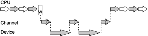
2.3.3 Input/Output systemIn contrast to other architectures that use I/O bus systems, the mainframe uses I/O channels. An I/O channel is a processor that manages the data movement between memory and external devices under the control of channel programs. In other words, I/O on the mainframe is managed independently of the CPUs. Architecturally, only the independent and overlapped execution aspects are specified and not whether a separate CPU is required for each real channel. For example, on the IBM zSeries machines, a single System Assist Processor (SAP) might control up to a hundred channels and the associated hardware interfaces. Design of I/OWe have mentioned that it is possible for a mainframe CPU to be consistently busy more than 90% of the time. This requires that the CPU be given a steady stream of work to do. One of the potential bottlenecks in some system designs is the I/O design. The central CPUs can process data at nanosecond speed. The rest of the computer system should be able to feed the CPUs information, and receive it from them, at the speed that they need it. Hence, there must be a balance between the CPUs, the memory, and the I/O. Let's take a look at data processing from the I/O perspective. The simple, early approach to I/O was the following: Send out requests for data to a device, wait for data to be returned (the job is said to enter a wait state), and then continue processing. This is illustrated in Figure 2-11. Figure 2-11. Simple I/O system design
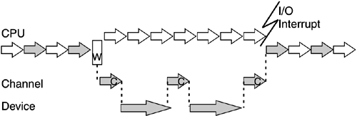
Figure 2-11 shows quite a gap in processing while the I/O device is busy. In order to keep the CPU busy, mainframe designers decided to use this gap for other processing. The CPU would continue with other waiting work until an I/O interrupt signaled that the I/O operation was complete (Figure 2-12). Figure 2-12. Mainframe I/O processing. The CPU can process other tasks while some tasks are waiting for I/O.
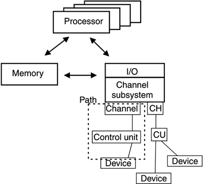
On early systems with 500 KB of real storage, three to five users (or programs) running simultaneously was the rule. As the CPU became faster, the idle time became significant again, as all programs were processed up to a point where they waited for I/O. It thus became possible for the CPU to load and initiate even more work. With the help of virtual memory (see 2.3.2, "Memory" in this chapter), it was possible to significantly increase CPU utilization. Over the years, further improvements were made to I/O handling. Notice the two large gaps on the middle line (channel) in Figure 2-12. This means that the channel could execute another channel program that talks to a different device. By contrast, on the bottom line (device) the middle gap is small; the device should not do anything else until this data action is processed. While Figure 2-12 shows the principle of how a program is interrupted to wait for I/O, it doesn't show the proportions of time. I/O from DASD typically takes five orders of magnitude longer than a CPU cycle. For example, if we were to slow down the CPU so that a cycle lasted one second, the I/O operation would take days. Over time, the mainframe's I/O system was optimized to keep feeding the CPUs data, allowing them to do other work while waiting for data. Mainframe I/O processingIn the S/360 computing systems, a channel decodes the channel program, which in turn is composed of CCWs. Channels are not the same as the physical cabling; rather, they are a logical construct. The path, on the other hand, is the actual physical path that data can take to a device, as illustrated in Figure 2-13. Figure 2-13. Mainframe I/O subsystem. Channels are connected to control units to which devices connect.
Each external device can be connected to one or more channels to allow for high bandwidth and reliability for data access on the external devices. Channels make it possible to overlap requests to a disk to connect as soon as it is not active elsewhere and check the existing data on the disk to determine if and when what type of data transfer may occur all done without any interaction with the CPU. Only upon completion of the channel program (or exception termination) is the CPU made aware of what has occurred. The CPU is not involved in the data movement. As shown in Table 2-2 , the mainframe I/O subsystem has evolved from an initial maximum of 8 channels. Each channel is capable of transferring data as needed between memory and external devices independently and coincidently with other channel and CPU access to memory. This capability allows for the high data transfer rates required to sustain multiprocessing activities on up to 16 CPUs.
|
EAN: 2147483647
Pages: 199
- Challenging the Unpredictable: Changeable Order Management Systems
- The Effects of an Enterprise Resource Planning System (ERP) Implementation on Job Characteristics – A Study using the Hackman and Oldham Job Characteristics Model
- Distributed Data Warehouse for Geo-spatial Services
- Healthcare Information: From Administrative to Practice Databases
- Development of Interactive Web Sites to Enhance Police/Community Relations