81.
7.2 Counter Design Procedure
This section begins our study of designing an important class of clocked sequential logic circuits-synchronous finite-state machines. Like all sequential circuits, a finite-state machine determines its outputs and its next state from its current inputs and current state. A synchronous finite-state machine changes state only on the clocking event.7.2.1 Introduction and an Example
Counter design is a good place for you to start understanding the design process for finite-state machines. Counters are the simplest possible finite-state machines. They typically have only a single input instructing them to count(often just the clock), and their outputs are nothing more than their current state.Three-Bit Up-Counter: State Transition Diagram Let's start with a simple counter, a 3-bit binary up-counter. We begin the design process by understanding how the counter is to operate. A convenient way to describe this is with a graphical specification called a state transition diagram.
The state transition diagram is a graph with nodes and directed arcs. Each node represents a unique state of the counter. A directed arc connects two nodes representing the present state and the next state. If the counter is in the state at the tail of the arc, it will advance to the state at the head of the arc at the next count request.
For the example design, we will dispense with a "count" input, and simply allow the counter to advance to the next state on each clock pulse.
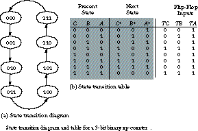
Figure 7.14(a) shows a state transition diagram for the example. The nodes are labeled with the counter state they represent, and the arcs connect the nodes in the sequence implemented by the counter. We can describe the behavior of any finite-state machine with a state transition diagram, although the diagrams are typically more complex than those for counters.
Three-Bit Up-Counter: State Transition Table An alternative formulation of the state transition diagram is the state transition table, which shows the present state with the next state. Each row corresponds to an arc in the state transition diagram. The state transition table for the up-counter is given in Figure 7.14(b).
Each bit of the state is held by a single storage element. In this example, the counter proceeds through eight states. To assign binary codes to these states, we need exactly three storage elements. We have named the storage elements C, B, and A, from the highest- to the lowest-order bit.
Three-Bit Up-Counter: Flip-Flop Choice The next step is to choose a kind of flip-flop to implement the counter's storage elements. A close look at the state transition table suggests that toggle flip-flops might be an attractive choice. In essence, A toggles on every clock pulse, B on every second clock pulse, and C on every fourth clock pulse. This is a binary counter, after all.
The rightmost column of the state transition table of Figure 7.14(b) shows the inputs that must be presented to toggle flip-flops to implement the desired state transitions. For example, consider the state transition from 011 to 100. To get toggle flip-flops to implement these state changes, we must set the toggle input of each flip-flop to one. The transition will take place on the appropriate clock edge after the toggle inputs are set.
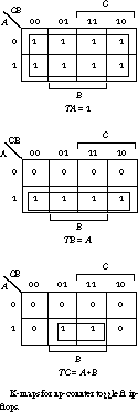
Three-Bit Up-Counter: Next-State Logic Our task now is to design combinational logic whose input is the current state of the counter and whose output is the toggle inputs to the state flip-flops. For this simple example, we can determine the logic just by examining the transition table. Flip-flop A toggles on each state transition, B toggles whenever A is asserted, and C toggles whenever A and B are asserted.
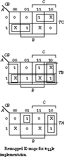
For more complex examples, we can view the transition table as a truth table that specifies the flip-flops' inputs as a function of C, B, and A. We would use standard K-map methods to obtain the reduced Boolean expressions. The K-maps for TC, TB, and TA are shown in Figure 7.15.
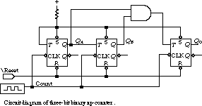
This leads immediately to the circuit design of Figure 7.16.
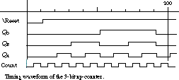
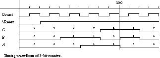
The timing waveform of this implementation is given in Figure 7.17.
7.2.2 Counters with More Complex Sequencing
The generalized design process consists of the following four steps:- Step 1: From the written specification of the counter, we first draw a state transition diagram that shows the counter's desired sequence.
- Step 2: We next derive the state transition table from the state -diagram, tabulating the current state with the next state in the count sequence. Each state bit is implemented by its own flip-flop.
- Step 3: We express each next-state bit as a combinational logic function of the current state bits.
Step 4: We choose a flip-flop for implementation. Then we must "remap" the next-state mapping derived in step 3 to obtain the desired behavior from the selected flip-flop. - Step 2: We next derive the state transition table from the state -diagram, tabulating the current state with the next state in the count sequence. Each state bit is implemented by its own flip-flop.
Example Generalized Counter Design To see this four-step process in action, let's look at another implementation of a counter. We will design a 3-bit counter that advances through the sequence 000, 010, 011, 101, 110, 000 and repeats. Not all of the possible combinations of the 3 bits represent a valid state. The unused states, 001, 100, and 111, can be used as don't-care conditions to simplify the logic.Step 1: Draw the state transition diagram. This is shown in Figure 7.18.
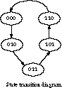
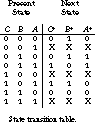
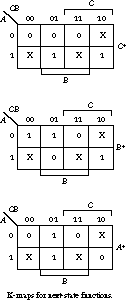
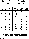
Figure 7.21 shows the toggle inputs needed to implement the state transitions of Figure 7.18.

For example, counter state 000 advances to 010, so the inputs to the toggle flip-flops should be 0 (don't toggle) for C, 1 (toggle) for B, and 0 (don't toggle) for A. Similarly, state 110 returns to 000. In this case, the control for C, B, A is toggle, toggle, don't toggle, respectively, or 110.
Reflecting this remapping of functions, the K-maps become those of Figure 7.23.
The minimized functions become

Figure 7.24 shows the component-level implementation, with its associated timing waveform in Figure 7.25. To reduce wiring complexity, we simply label input and output nets rather than draw them as wires. Two nets with the same label are understood to be connected. The proper sequencing through the states 000, 010, 011, 101, 110, 000 should be clear from the waveform.
[Top] [Next] [Prev]